Optimization of Spark Plasma Sintering Temperature Conditions for Enhancement of Thermoelectric Performance in Gas-Atomized Bi0.5Sb1.5Te3 Compound
Article information
Abstract
We fabricate fine (<20 μm) powders of Bi0.5Sb1.5Te3 alloys using a large-scale production method and subsequently consolidate them at temperatures of 573, 623, and 673 K using a spark plasma sintering process. The microstructure, mechanical properties, and thermoelectric properties are investigated for each sintering temperature. The microstructural features of both the powders and bulks are characterized by scanning electron microscopy, and the crystal structures are analyzed by X-ray diffraction analysis. The grain size increases with increasing sintering temperature from 573 to 673 K. In addition, the mechanical properties increase significantly with decreasing sintering temperature owing to an increase in grain boundaries. The results indicate that the electrical conductivity and Seebeck coefficient (217 μV/K) of the sample sintered at 673 K increase simultaneously owing to decreased carrier concentration and increased mobility. As a result, a high ZT value of 0.92 at 300 K is achieved. According to the results, a sintering temperature of 673 K is preferable for consolidation of fine (<20 μm) powders.
1. Introduction
The energy recovery from waste heat in an eco-friendly manner is attracting more and more interest due to the increased demand for fossil fuels and environmental matters. Thermoelectric materials (TE) can directly extract electricity from the waste heat which exists in heat engines, car exhausts, and pipes carrying hot fluids [1, 2]. The conversion efficiency of TE materials can be gauged by a dimensionless figure of merit, ZT = S2σT/ (κe + κL), where S, σ, κe, κL, and T are the Seebeck coefficient, the electrical conductivity, the electronic and lattice contributions to total thermal conductivity (κ) and the absolute temperature [3]. S, σ, and κe are strongly interrelated with electronic properties, while κL depends on the crystal structure and chemical bonding. Commercially available thermoelectric materials showed low ZT (≤ 1) which limits the large-scale applications of the thermoelectric devices. In order to get high ZT; several approaches have been developed and explored with theoretically and experimentally to enhance power factor S2σ through optimal doping/band engineering [3, 4] and reduce κL by nanostructuring or phonon scattering [5].
Bi2Te3-based alloys (e.g., Bi2Te3, Sb2Te3, Bi0.5Sb1.5Te3, and Bi2Se0.3Te2.7) are known as the most widely used thermoelectric materials at room temperature (300- 500 K) and lots of work has been done to improve their performance [6, 7]. Zheng et al. [8] proposed a melt-spinning combined with plasma activated sintering method to synthesize Bi0.5Sb1.5Te3 alloys, by which the maximum ZT reached 1.22 at 340 K. This was mainly due to an increase in phonon scattering by dislocations, nanoprecipitates, random distribution of grains and twin boundaries. Xu et al. [9] obtained a high ZT of 1.36 at 400 K by zone melting and hot deformation process. These combination processes induce a donor-like effect and point defects, which could enhance the electrical properties and reduce the lattice thermal conductivity. Poudel et al. [10] prepared BiSbTe alloy with ultra-fine particles and Te precipitates ranging from 5-30 nm by using ball milling and hot press process. Consequently, the peak ZT value reached 1.4 at 373 K by increased phonon scattering by defects and grain boundaries. Recently, the nanomaterials such as quantum dots [11], nanoplates [12], superlattices [13] and nanocomposites [14], showed high thermoelectric performance due to the reduction of lattice thermal conductivity by involving phonon scattering. The abovementioned processes take a long time and difficult to control for fabrication of thermoelectric alloys. The gasatomization is the alternative cost-effective process for the production of high purity thermoelectric alloys. The productivity (2 kg/min) of the TE powders has been significantly higher compared to other conventional fabrication processes [7, 15].
Consolidation of thermoelectric powders is also most important step to fabricate polycrystalline materials. Several reports on indicated that sintering process can modify the microstructure of the bulk material [16]. Among the above-described sintering techniques, the spark plasma sintering has been widely used due to the short densification time (<10 min) [17]. Recently, Park et al. [7] reported on the reliability verification large diameter SPS processed pellets (50 mm). The performance at different positions of the large diameter pellets exhibits nearly same, which suggest that gas-atomization and spark plasma sintering is an effective powder metallurgy process for large-scale production.
In this study, fine powder particles of the ternary Bi0.5Sb1.5Te3 alloy was fabricated by the gas-atomization process and subsequently consolidated at three different sintering temperatures using spark plasma sintering process. The gas-atomized fine powders were spherical shape and their sizes were in the range of 1 to 20 μm. We have investigated the effect of sintering temperature on electrical, thermal and mechanical properties. The Seebeck coefficient and electrical conductivity simultaneously increased for the sample SPS processed at 673 K.
2. Experimental procedure
High purity elemental granules Bi (99.99%), Sb (99.99%), and Te (99.99%) were purchased from Alfa Aesar Co. Ltd and were weighed according to the formula of Bi0.5Sb1.5Te3. The raw materials were melted at a temperature of 200°C above the melting point by high-frequency induction furnace under argon atmosphere in a graphite crucible. The detailed processing conditions were reported our previous work [15, 18]. The gas-atomizer has two cyclone chambers; one can collect coarse particles (< 200 μm) and another chamber can collect fine particles (< 20 μm). In this work, we have used fine particles to further investigation of thermoelectric properties. The collected powders were consolidated using spark plasma sintering at three different temperatures (573, 623 and 673 K) for 10 min under an axial pressure of 50 MPa in a 20-mm diameter die. The particle size distributions of the as-atomized powders were measured by laser diffraction technique using a Mastersizer-2000 particle size analyzer. The phase constituents of the powders and bulk samples were examined by x-ray diffraction technique using Rigaku diffractometer (MiniFlex- 600, Japan) with CuKα radiation (λ = 0.15418 nm). Vickers microhardness of the bulk samples was measured using micro Vickers hardness tester. The powder morphology and fracture surface analysis of bulk samples were characterized by scanning electron microscopy (SEMMIRA- LMH II (TESKAN)). The SPS-processed bulk samples were cut into rectangular pieces (3×3×12 mm3); then used to measure the Seebeck coefficient, electrical conductivity and power factor by thermoelectric power measuring system (TEP-1000, Seepel). Disks of 12.7 mm in and less than 2 mm thickness specimens were prepared for measurement of thermal properties. Thermal diffusivity (λ) and specific heat (Cp) were measured using the laser flash method with an LFA 457 system and Perkin Elmer DSC-8000 system, respectively. The bulk density (d) was measured by Archimedes principle. The total thermal conductivity was calculated according to the relation κ = λCpd. Hall carrier concentration (nc) and carrier mobility (μc) of bulk samples were measured using Hall measurement system (Ecopia, HMS-3000).
3. Results and discussion
Fig. 1 shows the typical morphology and size distribution of gas atomized Bi0.5Sb1.5Te3 powder. As can be seen in the Fig. 1(a), the powder particles produced by gasatomization appeared in a spherical shape with smooth surfaces. The powder sizes of atomizer second chamber are in the range between 1 to 20 μm. The log-normal size distributions of gas-atomized Bi0.5Sb1.5Te3 powders are shown in Fig. 1(b). The average diameter of fine powder particles was around 15 μm which consistent with SEM results.
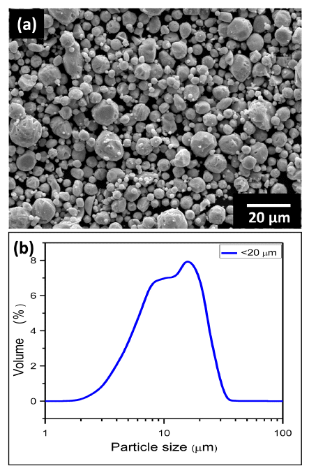
Fine powder morphology (a), and log normal size distribution (b) of the gas-atomized Bi0.5Sb1.5Te3 alloy.
Fig. 2(a, b) shows the x-ray diffraction patterns of gasatomized Bi0.5Sb1.5Te3 powder and bulk samples obtained at 573, 623 and 673 K. All the diffraction peaks for the powder and bulk samples were well matched with rhombohedral structure of Bi0.5Sb1.5Te3 phase (JCPDS#491713) having lattice parameters of a = 4.284 Å and c = 30.523 Å. In addition, the diffraction peak intensity was increased with increasing sintering temperature. The results indicating that the grain size can be varied with sintering temperatures.
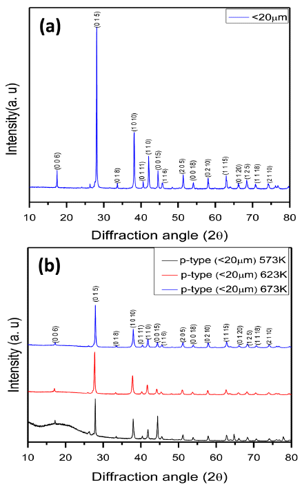
X-ray diffraction patterns of gas-atomized Bi0.5Sb1.5Te3 alloy; (a) powder and (b) bulk sample obtained at 573, 623 and 673 K.
The microstructural feature of the bulk samples plays an important role on the charge transport properties. Fig. 3 shows the SEM micrographs observed on the fracture surfaces of the Bi0.5Sb1.5Te3 samples prepared at different sintering temperatures. It is obvious that the grain size increased with increasing sintering temperature, and there is no porosity was observed. The obtained average grain size was round 20, 27 and 33 μm for the samples sintered at 573 K, 623 K, and 673 K, respectively.
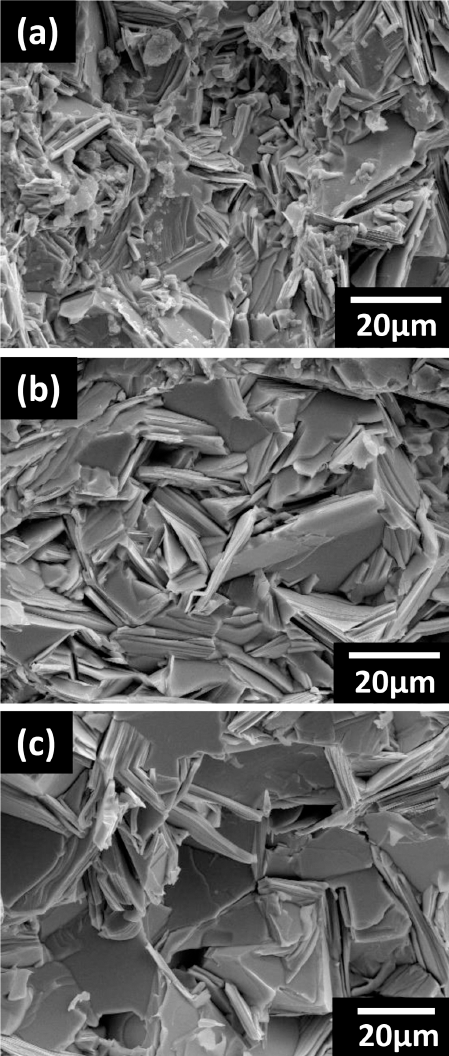
SEM fracture surface of spark plasma sintered Bi0.5Sb1.5Te3 alloys with different temperature (a) 573 K, (b) 623 K and (c) 673 K.
The relative densities of spark plasma sintered Bi0.5Sb1.5Te3 samples with different sintering temperatures (573, 623 and 673 K) are presented in Fig. 4(a). The relative density increased from 97.7% to 99.9% with increasing sintering temperature. The micro Vickers hardness of spark plasma sintered Bi0.5Sb1.5Te3 samples with different sintering temperatures (573, 623 and 673 K) are presented in Fig. 4(b). It can be seen in the figure, the hardness values are slightly increased with decreasing sintering temperature from 673 K to 573 K, due to the increased grain boundaries. The high density of grain boundaries can inhibit the crack propagation with response to the indentation load. The maximum hardness reached 79.5 Hv for the sample sintered at 573 K. The achieved a hardness of the sintered samples was higher or comparable with previously reported [7, 18].
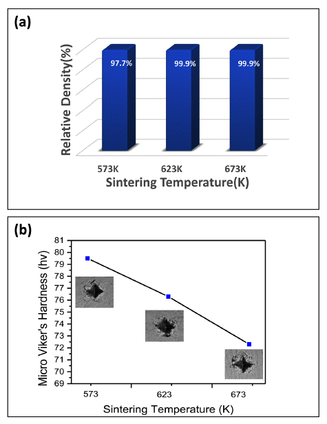
Relative density (a) and Vickers microhardness (b) of spark plasma sintered Bi0.5Sb1.5Te3 samples with different sintering temperatures.
Fig. 5 shows the temperature dependence of electrical conductivity, Seebeck coefficient, carrier concentration and mobility, power factor for the samples prepared at different sintering temperatures. As shown in Fig. 5(a), the electrical conductivity of all the sintered samples decreased with increasing measuring temperature, indicating a degenerate semiconducting material behavior. The electrical conductivity (σ) is directly proportional to the carrier concentration (nc) and mobility (μc), described according to the relation σ = nceμc, where e is the electronic charge. As shown in Fig. 5(c), the room-temperature carrier concentration decreased with increasing sintering temperature. The low carrier mobility was achieved for the sample sintered at 573 K, mainly attributed to the scattering of electrons by fine grains and carrier-carrier scattering [19].
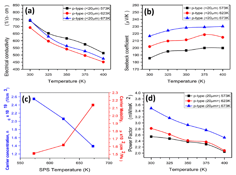
Temperature dependence of (a) Electrical conductivity, (b) Seebeck coefficient, (c) Carrier concentration and mobility, and (d) Power factor for the samples prepared at different sintering temperatures.
The electrical conductivity values decreased with increasing sintering temperature and then again tend to increase with further increasing sintering temperature. This is attributed with variety of the carrier concentration and mobility at the same time. The sample sintered at 573 K exhibits higher electrical conductivity due to the high carrier concentration.
Fig. 5(b) shows the temperature dependence of Seebeck coefficient for the samples prepared at different sintering temperatures. The Seebeck coefficient value for all the samples shows positive, which indicates that holes are playing a major role in the transportation. The Seebeck coefficient at 300K increased significantly from about 185 to 217 μV/K with increasing sintering temperature from 573 K to 673 K. The enhancement of Seebeck coefficient may be due to the easy Te diffusion into matrix with increasing sintering temperature [20]. In addition, the Seebeck coefficient (S) is strongly depends on the scattering parameter (γ) at a given temperature and the carrier concentration (nc) as described in Eq. (1) as follows [21],
The scattering occurs readily at the fine grains and grain boundaries. The sample sintered at 573 K exhibited fine microstructure, while the carrier concentration also higher. As a result, the Seebeck coefficient for the sample sintered at 573 K was decreased. In contrast, the Seebeck coefficient for the sample sintered at 673 K was increased corresponding to decrease in the carrier concentration and diffusion of Te into matrix.
Fig. 5(d) shows the temperature dependence of power factor for the samples prepared at different sintering temperatures. The power factor value increased with increasing sintering temperature from 573 to 673 K. The electrical conductivity and Seebeck coefficient simultaneously increased for the sample sintered at 673 K. As a result, the power factor reached a maximum value of 3.49×10⁻³ Wm-1K-2 for the sample sintered at 673 K, which is higher than previously reported results [22].
The temperature dependence of thermal transport properties of the samples prepared at different sintering temperatures is presented in Fig. 6. The total thermal conductivity (κ) is a combination of lattice thermal conductivity (κL), and electronic thermal conductivity (κe). Generally, the electronic thermal conductivity can be estimated using Wiedemann-Franz law (κe = LσT), where L = 1.5×10⁻⁸ V2K-2 in non-degenerate semiconductors [13]. As shown in Fig. 6(a), the total thermal conductivity decreased with decreasing sintering temperature. The κ becomes smaller and reaches the minimum value of 1.12 W/mK at 325 K for the sample sintered at 573 K. The lattice thermal conductivity gives a major contribution to total thermal conductivity (Fig. 6(b)). The variation of the lattice thermal conductivity is consistent with the total thermal conductivity. The reduction of thermal conductivity can be ascribed to the enhancement of phonon scattering by the high density of grain boundaries. The electronic thermal conductivity increased with decreasing sintering temperature (Fig. 6(c)).
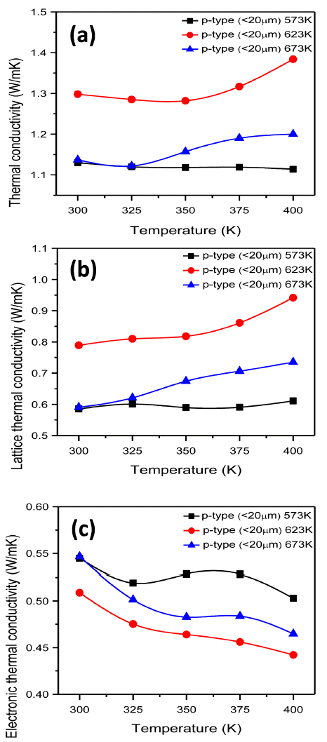
Temperature dependence of (a) Thermal conductivity, (b) Lattice thermal conductivity (c) Electronic thermal conductivity for the samples prepared at different sintering temperatures.
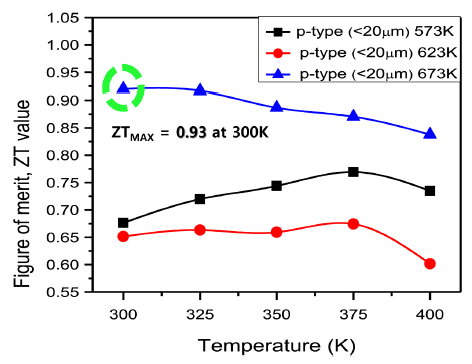
Fig. 7 shows the temperature dependence of dimensionless figure of merit (ZT) for the samples prepared at different sintering temperatures. The maximum ZT values for the samples sintered at 573, 623 and 673 K are 0.77 at 375 K, 0.67 at 375 K and 0.92 at 300 K, respectively. Interestingly, the enhanced ZT value for the sample sintered at 673 K was mainly due to the enhanced Seebeck coefficient, electrical conductivity, and reduction of thermal conductivity. Based on the results, we can conclude that the optimization temperature was 673 K for the consolidation of fine gas atomized powders. Nevertheless, the optimization of sintering temperature for the fine (< 20 μm) gas atomized powders could helpful for the development of room temperature thermoelectric applications.
4. Conclusions
In this work, we fabricated fine (< 20 μm) powders of Bi0.5Sb1.5Te3 alloys using large-scale production method, and subsequently consolidated at different temperatures (573, 623, and 673 K) using spark plasma sintering process. The effect of sintering temperature on the microstructure, mechanical and thermoelectric properties in Bi0.5Sb1.5Te3 alloys have been investigated systematically. The result indicates that electrical conductivity and Seebeck coefficient simultaneously increased due to the decreased in carrier concentration and increase mobility for the sample sintered at 673 K. The thermal conductivity has also been decreased due to the enhanced scattering of phonons by grain boundaries. As a result, a high ZT value of 0.92 at 300 K was achieved. We can conclude that the optimization temperature was 673 K for the enhancement of thermoelectric performance. Moreover, mechanical properties significantly increased with decreasing sintering temperature due to increased grain boundaries.
Acknowledgments
This work was supported by the Korea Institute of Energy Technology Evaluation and Planning (KETEP) granted financial resource from the Ministry of Trade, Industry & Energy, Republic of Korea (No.20152020001210).
