- [Korean]
- Recent Studies on Area Selective Atomic Layer Deposition of Elemental Metals
-
Min Gyoo Cho, Jae Hee Go, Byung Joon Choi
-
J Powder Mater. 2023;30(2):156-168. Published online April 1, 2023
-
DOI: https://doi.org/10.4150/KPMI.2023.30.2.156
-
-
4,123
View
-
102
Download
-
2
Citations
-
 Abstract Abstract
 PDF PDF
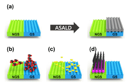
The semiconductor industry faces physical limitations due to its top-down manufacturing processes. High cost of EUV equipment, time loss during tens or hundreds of photolithography steps, overlay, etch process errors, and contamination issues owing to photolithography still exist and may become more serious with the miniaturization of semiconductor devices. Therefore, a bottom-up approach is required to overcome these issues. The key technology that enables bottom-up semiconductor manufacturing is area-selective atomic layer deposition (ASALD). Here, various ASALD processes for elemental metals, such as Co, Cu, Ir, Ni, Pt, and Ru, are reviewed. Surface treatments using chemical species, such as self-assembled monolayers and small-molecule inhibitors, to control the hydrophilicity of the surface have been introduced. Finally, we discuss the future applications of metal ASALD processes. -
Citations
Citations to this article as recorded by  - Ultrafast Synthesis of Molybdenum Disulfide via Flashlamp Annealing
Chan Hyeon Yang, Jaehak Lee, Jung Hwan Park
Journal of Powder Materials.2025; 32(6): 509. CrossRef - Selective Atomic Layer Deposition of Co Thin Films Using Co(EtCp)2 Precursor
Sujeong Kim, Yong Tae Kim, Jaeyeong Heo
Korean Journal of Materials Research.2024; 34(3): 163. CrossRef
|