Search
- Page Path
- HOME > Search
- [Korean]
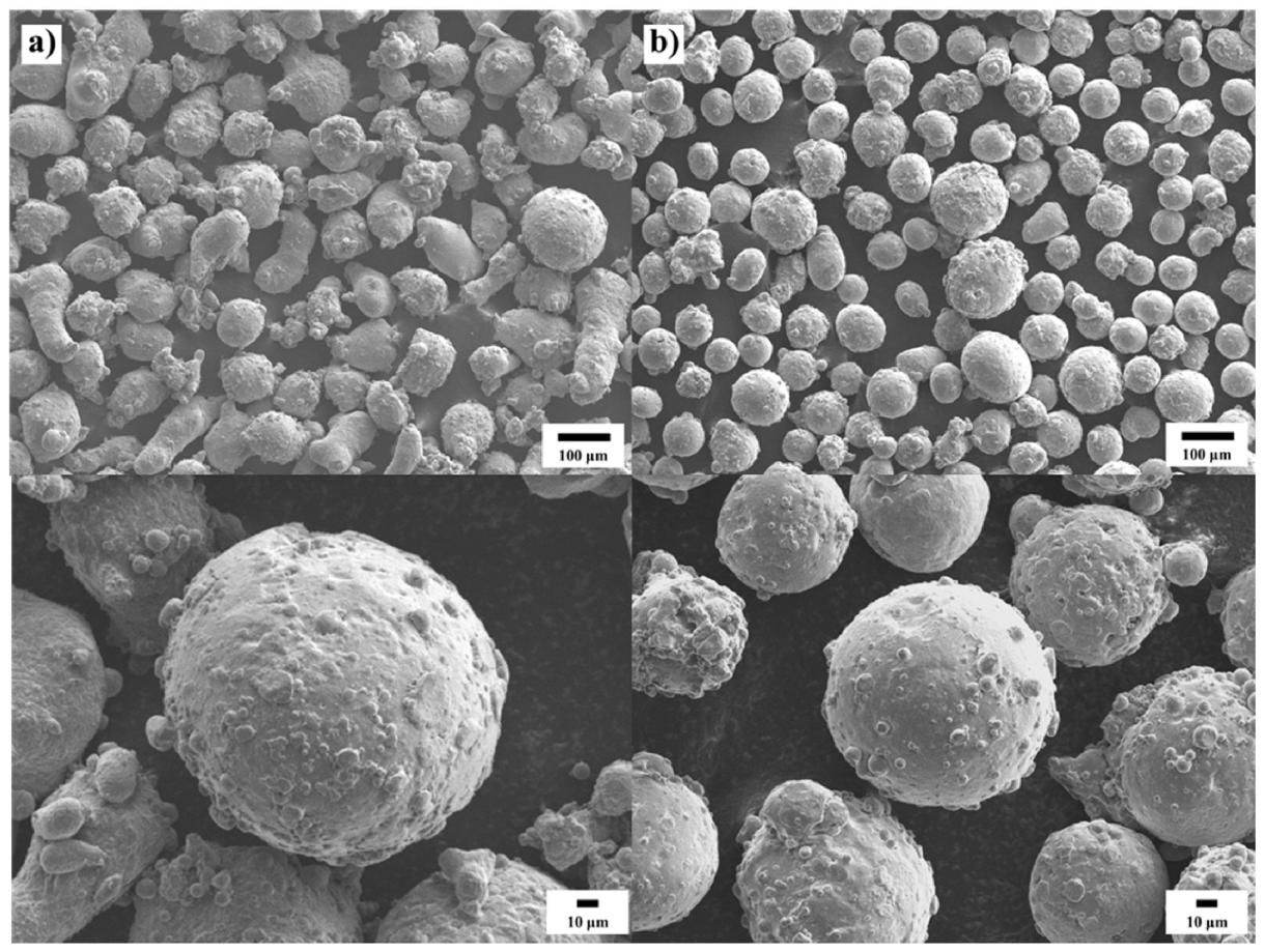
- Combinatorial Experiment for Al-6061 and Al-12Si alloy Based on Directed Energy Deposition (DED) Process
- Seoyeon Jeon, Suwon Park, Yongwook Song, Jiwon Park, Hyunyoung Park, Boram Lee, Hyunjoo Choi
- J Powder Mater. 2023;30(6):463-469. Published online December 1, 2023
- DOI: https://doi.org/10.4150/KPMI.2023.30.6.463

- 2,214 View
- 47 Download
- 4 Citations
-
 Abstract
 PDF
PDF Aluminum alloys, known for their high strength-to-weight ratios and impressive electrical and thermal conductivities, are extensively used in numerous engineering sectors, such as aerospace, automotive, and construction. Recently, significant efforts have been made to develop novel aluminum alloys specifically tailored for additive manufacturing. These new alloys aim to provide an optimal balance between mechanical properties and thermal/ electrical conductivities. In this study, nine combinatorial samples with various alloy compositions were fabricated using direct energy deposition (DED) additive manufacturing by adjusting the feeding speeds of Al6061 alloy and Al-12Si alloy powders. The effects of the alloying elements on the microstructure, electrical conductivity, and hardness were investigated. Generally, as the Si and Cu contents decreased, electrical conductivity increased and hardness decreased, exhibiting trade-off characteristics. However, electrical conductivity and hardness showed an optimal combination when the Si content was adjusted to below 4.5 wt%, which can sufficiently suppress the grain boundary segregation of the α- Si precipitates, and the Cu content was controlled to induce the formation of Al2Cu precipitates.
-
Citations
Citations to this article as recorded by- Development of Aluminum Alloys for Additive Manufacturing Using Machine Learning
Sungbin An, Juyeon Han, Seoyeon Jeon, Dowon Kim, Jae Bok Seol, Hyunjoo Choi
Journal of Powder Materials.2025; 32(3): 202. CrossRef - Trends in Materials Modeling and Computation for Metal Additive Manufacturing
Seoyeon Jeon, Hyunjoo Choi
journal of Korean Powder Metallurgy Institute.2024; 31(3): 213. CrossRef - The Challenges and Advances in Recycling/Re-Using Powder for Metal 3D Printing: A Comprehensive Review
Alex Lanzutti, Elia Marin
Metals.2024; 14(8): 886. CrossRef - Microstructural Effects on the Mechanical Properties of Ti-6Al-4V Fabricated by Direct Energy Deposition
Juho Kim, Seoyeon Jeon, Hwajin Park, Taeyoel Kim, Hyunjoo Choi
Journal of Powder Materials.2024; 31(4): 302. CrossRef
- Development of Aluminum Alloys for Additive Manufacturing Using Machine Learning
- [Korean]
- Effect of WC Particle Size on the Microstructure, Mechanical and Electrical Properties of Ag/WC Sintered Electrical Contact Material
- Soobin Kim, So-Yeon Park, Jong-Bin Lim, Soon Ho Kwon, Kee-Ahn Lee
- J Powder Mater. 2023;30(3):242-248. Published online June 1, 2023
- DOI: https://doi.org/10.4150/KPMI.2023.30.3.242

- 1,128 View
- 7 Download
- 1 Citations
-
 Abstract
 PDF
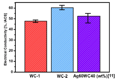
PDF The Ag/WC electrical contacts were prepared via powder metallurgy using 60 wt% Ag, 40 wt% WC, and small amounts of Co3O4 with varying WC particle sizes. After the fabrication of the contact materials, microstructure observations confirmed that WC-1 had an average grain size (AGS) of 0.27 μm, and WC-2 had an AGS of 0.35 μm. The Ag matrix in WC-1 formed fine grains, whereas a significantly larger and continuous growth of the Ag matrix was observed in WC-2. This indicates the different flow behaviors of liquid Ag during the sintering process owing to the different WC sizes. The electrical conductivities of WC-1 and WC-2 were 47.8% and 60.4%, respectively, and had a significant influence on the Ag matrix. In particular, WC-2 exhibited extremely high electrical conductivity owing to its large and continuous Ag-grain matrix. The yield strengths of WC-1 and WC-2 after compression tests were 349.9 MPa and 280.7 MPa, respectively. The high yield strength of WC-1 can be attributed to the Hall–Petch effect, whereas the low yield strength of WC-2 can be explained by the high fraction of high-angle boundaries (HAB) between the WC grains. Furthermore, the relationships between the microstructure, electrical/mechanical properties, and deformation mechanisms were evaluated.
-
Citations
Citations to this article as recorded by- Enhanced Epoxy Composites Reinforced by 3D-Aligned Aluminum Borate Nanowhiskers
Hyunseung Song, Kiho Song, Haejin Hwang, Changui Ahn
Materials.2024; 17(19): 4727. CrossRef
- Enhanced Epoxy Composites Reinforced by 3D-Aligned Aluminum Borate Nanowhiskers
- [Korean]
- Research Trends in Powder Materials for Solution-based Transparent Conducting Electrode
- Bon-Ryul Koo, Hyo-Jin Ahn
- J Korean Powder Metall Inst. 2017;24(2):153-163. Published online April 1, 2017
- DOI: https://doi.org/10.4150/KPMI.2017.24.2.153

- 901 View
- 4 Download
- 1 Citations
-
 Abstract
 PDF
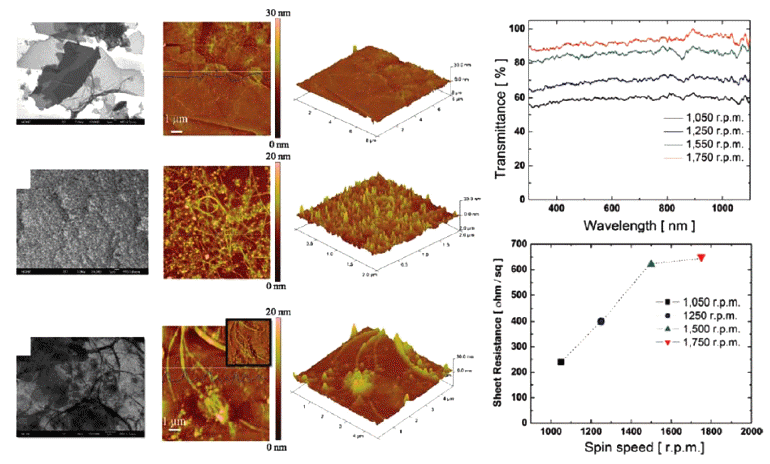
PDF Transparent conducting electrodes (TCEs) are attracting considerable attention as an important component for emerging optoelectronic applications such as liquid crystal displays, touch panels, and solar cells owing to their attractive combination of low resistivity (< 10-3 Ω cm) and high transparency (>80%) in the visible region. The solutionbased process has unique properties of an easy fabrication procedure, scalability, and low cost compared to the conventional vacuum-based process and may prove to be a useful process for fabricating TCEs for future optoelectronic applications demanding large scale and flexibility. In this paper, we focus on the introduction of a solution-based process for TCEs. In addition, we consider the powder materials used to fabricate solution-based TCEs and strategies to improve their transparent conducting properties.
-
Citations
Citations to this article as recorded by- Electrically conductive and anti-corrosive coating on copper foil assisted by polymer-nanocomposites embedded with graphene
Han Kim, Hyemin Lee, Hyo-Ryoung Lim, Hong-Baek Cho, Yong-Ho Choa
Applied Surface Science.2019; 476: 123. CrossRef
- Electrically conductive and anti-corrosive coating on copper foil assisted by polymer-nanocomposites embedded with graphene
TOP
 KPMI
KPMI


 First
First Prev
Prev


