
Articles
- Page Path
- HOME > J Korean Powder Metall Inst > Volume 21(5); 2014 > Article
-
ARTICLE
Pt 나노분말이 분산된 SiO2 박막의 구조 및 전기적 특성 제어 - 이재호, 신인주, 이성우, 김형철, 최병준*
- Controlling Structural and Electrical Properties of Pt Nanopowder-Dispersed SiO2 Film
- Jae Ho Lee, In Joo Shin, Sung Woo Lee, Hyeong Cheol Kim, Byung Joon Choi*
-
Journal of Korean Powder Metallurgy Institute 2014;21(5):355-359.
DOI: https://doi.org/10.4150/KPMI.2014.21.5.355
Published online: September 30, 2014
서울과학기술대학교 신소재공학과
Department of Materials Science and Engineering, Seoul National University of Science and Technology, Seoul 139-743, Korea
- *Corresponding Author : Byung Joon Choi, TEL: +82-2-970-6641, FAX: +82-2-973-6657, E-mail: bjchoi@seoultech.ac.kr
• Received: September 11, 2014 • Revised: September 18, 2014 • Accepted: September 19, 2014
© Korean Powder Metallurgy Institute
This is an Open-Access article distributed under the terms of the Creative Commons Attribution Non-Commercial License (http://creativecommons.org/licenses/by-nc/3.0) which permits unrestricted non-commercial use, distribution, and reproduction in any medium, provided the original work is properly cited.
- 923 Views
- 2 Download
Abstract
- Pt nanopowder-dispersed SiO2 (SOP) films were prepared by RF co-sputtering method using Pt and SiO2 targets in Ar atmosphere. The growth rate and Pt content in the film were controlled by means of manipulating the RF power of Pt target while that of SiO2 was fixed. The roughness of the film was increased with increasing the power of Pt target, which was mainly due to the increment of the size and planar density of Pt nanopowder. It was revealed that SOP film formed at 10, 15, 20 W of Pt power contained 2.3, 2.7, and 3.0 nm of spherical Pt nanopowder, respectively. Electrical conductivity of SOP films was exponentially increased with increasing Pt power as one can expect. Interestingly, conductivity of SOP films from Hall effect measurement was greater than that from DC I-V measurement, which was explained by the significant increase of electron density.
- 모제가 되는 절연 산화막에 마이크로 미터 크기 이하의 금속 분말을 균일하게 분산시킨 복합 박막 소재는 광학적, 전자기적, 열적, 열전적, 기계적 특성 등 재료의 다양한 특 성을 제어하는 것이 가능하다[1]. 세라믹과 금속의 합성어 인 서멧(ceramic + metal = cermet)으로도 알려진 이 소재 는 순수한 금속에 비해 훨씬 높은 저항과, 비교적 낮은 PTCR(positive temperature coefficient of resistivity) 특성 으로 인해 전기 저항체로 쓰여 왔다.
- 동결 건조법[2], 습식 합성법[3-6], 물리 기상 증착법 (PVD; physical vapor deposition) 또는 분자선 에피택시 (MBE; molecular beam epitaxy) 증착법과 후속 열처리를 이용한 응집 (agglomeration) 방법[7-10], 고전압 이온 건 (gun)을 이용한 이온 임플란테이션(ion implantation)[11, 12], 멀티 소스 또는 타겟을 사용한 co-evaporation과 코스퍼터 링 (co-sputtering) 방법[1, 13, 14] 등 다양한 방법을 사용해 나노 크기의 금속 분말을 산화막에 균일하게 분산시킬 수 있다.
- 최근에는 Au, Ni, Pt, Ir, Co 등의 금속 물질 또는 Si, Ge 등의 반도체 물질이 1-10 nm 크기로 분산된 산화막을 이 용해 나노전자소자(nanoelectronics)에 응용하고자 하는 연 구가 이루어지고 있다. 대표적으로 CTF(charge trap flash) 메모리[6, 7, 10, 15-17], 저항변화 메모리(ReRAM; resistance random access memory)[4, 8, 9, 13, 14, 18] 등은 이러한 금 속 나노 물질이 포함된 산화막을 사용한 차세대 비휘발성 메모리로써, NAND flash 메모리나 DRAM(dynamic RAM)과 같은 현재의 메모리를 대체하고자 하는 많은 노 력이 이루어져 왔다.
- 본 연구에서는 코스퍼터링 방법을 이용해 금속 나노분 말의 함유량과 분말의 크기를 제어하고자 했다. 투과전자 현미경을 이용해 미세 구조를 관찰하고, Hall 효과 측정을 통해 전기 전도도를 측정함으로써, 이 복합 소재의 미세 구조와 전기적 특성의 연관성을 밝히고자 한다.
서 론
- 스퍼터링 증착 장비(AJA international, 미국)를 이용한 코스퍼터링을 위해 그림 1(a)와 같이 Pt(99.99%), SiO2 (99.5%) 두 종류의 타겟을 사용했다. 절연성을 갖는 SiO2 타겟과 전도성이 높은 Pt 타겟 모두 RF(radio frequency) 모드를 사용하는 RF sputtering을 사용했다. 증착은 Ar(순 도 99.999%) 16 SCCM을 흘려 주어 챔버 내 압력을 3 mTorr로 일정하게 유지한 상태에서 진행되었다. Pt가 분산 된 SiO2 (SOP) 박막의 증착 속도와 Pt 분율은 각각 SiO2 타 겟과 Pt 타겟의 RF 출력을 이용해 조절했다. SOP 박막의 증 착 속도는 알파 스텝 프로파일로미터(α-step profilometer)와 엘립소미터(ellipsometer)를 사용해서 측정했다.
- (a) Schematics of RF co-sputtering system with Pt and SiO2 target (off-axis), (b) variation in the thickness as a function of deposition time, where the slope of the linear fitting is considered as a growth rate of SOP and SiO2 films.
- 원자 힘 현미경(AFM; atomic force microscopy, DI- 3000, 미국)을 사용해 SOP 박막의 Pt 함량에 따른 표면 형 상 변화를 관찰했다. 투과전자현미경(TEM; Transmission electron microscopy, Jeol 3000-F, 일본)을 사용해 SOP 복 합 박막의 미세 구조를 관찰했다. Pt 나노분말의 크기를 측정하기 위해 저각 X-ray 산란(SAXS; Small angle X-ray scattering)법을 이용했다. 빔 소스로는 스탠포드 선형 가속 기 연구소(SLAC; Stanford Linear Accelerator Center)의 빔라인 SSRL 4-2를 사용했고, 이 때 입사 빔 에너지는 8.3 keV, 이에 따른 빔의 파장은 0.13 nm, 입사각은 0.5° 였다. SOP 시료의 전하 농도 및 전하 이동도를 측정하기 위해 Hall effect measurement 장치(HMS-3000, 에코피아, 한국) 를 사용했고, 종방향의 전기적 특성을 측정하기 위해 metal-SOP-metal capacitor 형태의 소자를 제작하고 반도 체 파라미터 분석 장비(HP-4156, Agilent, 미국)를 이용해 quasi-static (DC) I (전류)-V (전압) 특성을 분석했다. 모든 전기적 특성 측정은 상온에서 이루어졌다.
실험방법
Fig. 1.
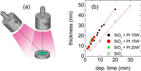
- 코스퍼터링을 이용한 SOP 박막 성장을 위해 Pt 타겟에 가해지는 RF 출력 조건을 변화 시켜, 증착 시간에 따른 박 막의 두께를 그림 1(b)에 나타냈다. SiO2 타겟의 RF 출력 은 180 W로 고정 시킨 상태에서 Pt 출력을 각각 10, 15, 20 W로 증가시켰다. 비교를 위해 Pt 타겟이 활성화되지 않은 상태에서 SiO2 180 W를 가한 채 동일한 증착 조건 으로 SiO2 박막을 증착했다. 그 결과 각 조건에서 증착 시 간에 따라 선형적으로 박막의 두께가 증가하는 것을 확인 할 수 있다. 각각의 그래프를 선형근사 시킨 기울기가 각 조건에서의 박막의 성장 속도에 해당된다. 표 1에는 선형 근사로부터 얻은 각 조건에서의 박막 성장 속도를 나타냈 다. Pt 출력에 따라 박막의 성장 속도가 0.11 nm/W로 거 의 선형적으로 증가하는 것을 알 수 있다. 즉, Pt 출력을 조절해 Pt의 SOP 복합막 내 함유량을 비교적 정확하게 조 절할 수 있었다. 표 1에는 RBS (Rutherford backscattering spectrometry) 분석을 통해 얻은 SOP 박막 내 Pt 함유량을 양이온 비율 (Pt%/(Si%+Pt%))로 나타냈다.
- Growth rate, Pt content, and the size of Pt nanopowders in SOP and SiO2 films
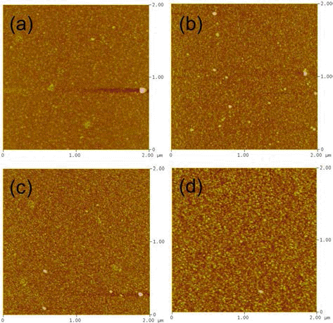
- 그림 2(a)-(d)에는 SiO2 박막과 SOP 박막의 Pt 출력에 따른 표면 형상 변화를 AFM으로 측정한 결과로 나타냈 다. Pt 함량이 크게 증가했음에도 전체적으로 비교적 평탄 한 표면 형상을 유지했고, 표면 거칠기는 rms (root-meansquare) 거칠기 값이 0.69 (SiO2), 0.86 (SOP-10W), 0.97 (SOP-15W), 1.22 nm (SOP-20W)로 점차 증가하는 양상을 볼 수 있었다. 이는 Pt 함량이 증가하면서 Pt 나노분말의 크기 증가와 함께 단위면적당 개수(면밀도) 역시 증가했기 때문인 것으로 생각된다.
- AFM image of (a) SiO2 27 nm, (b) SOP-10W 27 nm, (c) SOP-15W 22 nm, and (d) SOP-20W 22 nm. Rms roughness of the film was 0.69, 0.86, 0,97, and 1.22 nm, respectively.
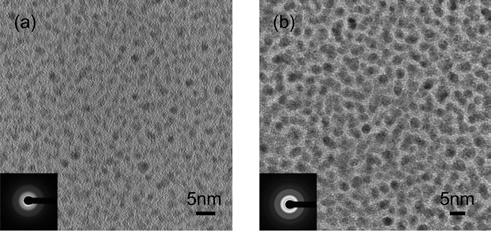
- SOP 복합막의 미세 구조를 관찰하기 위해 메쉬(mesh) 가 있는 TEM용 Cu 그리드 (grid) 상에 직접 기른 SOP- 10W와 20W 조건으로 성장시킨 복합막의 평판 TEM 사 진을 그림 3(a) (b)에 각각 나타냈다. 비정질의 SiO2 모제 (matrix)에 결정화가 이루어진 Pt 나노분말이 고르게 분포 하고 있는 미세 구조를 고분해능 TEM 사진을 통해 확인 할 수 있었다. 입도 분석을 통해 Pt 10W와 20W 조건에서 성장시킨 SOP 복합막은 각각 평균 2.1 nm와 3.3 nm 크기 를 갖는 결정 분말들이 존재하는 것을 알 수 있었다. 특히, 전자회절 분석을 통해 SOP-10W에 비해 20W 복합막에서 Pt 나노분말 다결정질의 링 회절 패턴이 보다 선명하게 나 타나는 것을 그림 3(a) (b)의 좌측 하단에 삽입된 전자회 절 패턴에서 확연히 볼 수 있다.
- Plan-view TEM image of (a) SOP-10W and (b) SOP- 20W film, respectively. Each inset figure is electron diffraction pattern.
- SOP 복합막의 Pt 나노분말의 크기와 분포를 분석하기 위해 저각 산란 실험 (SAXS)을 수행했다. Si 기판에 성장 시킨 200 nm 두께의 SOP-10W, 15W, 20W 복합막과 SiO2 박막에 그림 4(a)와 같이 0.5° 각도로 전자파 (λ=0.13 nm) 를 입사 시킨 후 나노분말에 의해 산란되어 나오는 전자 파를 검출했다. 이 때 평판 검출기에서 검출된 산란 패턴 으로 나타나는, 역격자 공간에서 투과파 (O)에 대한 산란 파의 거리에 해당하는 Q(/nm)에 대한 정보를 이용해 산란 입자의 형태와 크기를 알 수 있다[19]. 그림 4(a) 우측에 나타난 대칭적인 반원 형태의 산란 패턴은 SOP 복합막에 서 나온 것으로, 산란을 일으킨 입자가 구형을 이룬다는 것을 의미한다. 그림 4(b)에는 각 시편에서 얻은 Q값에 따 른 산란파의 세기를 나타냈다. 이 때의 세기는 산란 평면 에서 동일한 반지름을 갖는 Q값에 따른 세기를 모두 더한 값이다. 이 Q값에 대한 정보를 이용해 나노분말의 크기와 분포에 대한 정보를 얻을 수 있다. SiO2는 산란에 의한 peak이 검출되지 않아서 산란을 일으키는 수 nm 크기의 산란 인자가 존재하지 않는 비정질 상태로 밝혀졌다. 이에 반해 SOP 복합막은 비교적 뚜렷한 산란 peak들이 존재하 는 것을 볼 수 있다. 각각의 SOP 시료에서 가장 강한 산 란 peak이 보이는 Q값을 이용해 2π/Q값을 산출하면 산란 을 일으킨 나노분말의 크기를 알 수 있다. 표 1에 나타낸 바와 같이 2.33, 2.65, 2.99 nm로 Pt 출력이 증가함에 따라 나노분말 입자의 크기가 점진적으로 증가하는 것을 볼 수 있었다. 또한 Pt 출력이 높아질수록 산란 강도가 증가하는 것으로부터 나노분말의 밀도와 크기가 보다 균일해지는 것을 알 수 있었다.
- (a) Schematics of SAXS analysis on SOP films, where incident beam is scattered by Pt nanopowders dispersed in SiO2 matrix. Scattering pattern represents the shape and size of the nanopowders. (b) SAXS spectra of SOP and SiO2 films, where the most probable size of the nanopowders were estimated to 2.33 (SOP-10W), 2.65 (SOP-15W), and 2.99 nm (SOP-20W).
- SOP 복합막의 전기적 성질을 알아 보기 위해 Hall 효과 측정법과 DC I-V 특성 측정의 두 가지 방법을 사용했다. 먼저 Hall 효과 측정에서는 약 200 nm 두께의 SOP 박막 (SOP-10, 15, 20W)에서 Hall 계수 및 면저항으로부터 단 위 면적당 전자 농도(electron density, n)와 전자 이동도 (mobility, μ)를 검출할 수 있었다. 그림 5에는 SOP 복합막 의 Pt 출력에 따른 전자 농도 (좌)와 이동도 (우)를 나타냈 다. Pt 출력에 따라 Pt 함유량이 증가하면서 전자 농도가 크게 증가하는 것을 볼 수 있다. 그러나 전자의 이동도는 Pt 함유량이 증가할 때 오히려 소량 감소하는 경향을 보였다. 이는 Pt 함량이 증가함에 따라 전자 농도가 크게 증가하면 서 전자 간 충돌이 많아졌기 때문인 것으로 해석 된다.
- Variation in the electron density, n (cm−3) and mobility, μ (cm2/Vs) of SOP films as a function of Pt power (i.e. Pt content).
- 그림 6에는 반도체 파라미터 분석 장비로 측정한 DC I -V 특성을 박막의 두께와 전극의 면적으로 환산한 J (전류 밀도) - E(전기장) 특성 곡선을 나타냈다. 낮은 전압 영역 에서 절연성이 매우 우수한 SiO2 박막에 비해 Pt 나노분 말이 분산된 SOP 복합막은 전기 전도성이 크게 향상된 결 과를 나타냈다. Pt 출력이 증가함에 따라 Pt 나노분말의 크기는 크게 증가하지 않았지만, Pt 조성이 약 2.2 배 증 가했기 때문에(표 1 참고) SOP-20W의 경우 전기 전도성 이 SOP-10W나 SOP-15W에 비해서도 크게 향상된 것을 볼 수 있다. 이 결과로부터 Pt 나노분말의 크기도 물론 전 도성에 중요한 영향을 미칠 것으로 생각되지만, 나노분말 간의 거리가 감소할 경우 전자의 터널링 현상에 의존하는 전기 전도성이 급격히 증가하는 것으로 해석할 수 있다 [1, 11, 14, 20]. 나아가서는 Pt 나노분말 간의 거리와 터널 링에 따른 전기 전도성에 대한 보다 정확한 전기 전도 기 구가 필요한 것으로 생각된다.
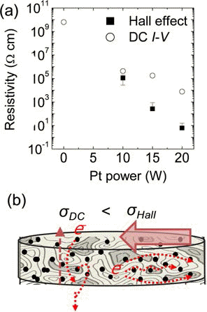
- 한편, Hall 효과 측정으로부터의 비저항과 J-E 특성으로 얻은 비저항을 비교해 보면, 그림 7(a)에 나타낸 바와 같 이 후자의 경우 비저항이 훨씬 더 높은 것을 볼 수 있다. 이를 설명하기 위해 그림 7(b)와 같은 모식도를 나타냈다. SOP-15W, 20W의 경우 Hall 효과에 의한 비저항이 크게 낮아졌는데 이는 Pt 함유량이 증가하면서 주입 또는 생성 되는 전자 농도가 크게 증가한 것이 주요한 원인으로 생 각 된다. 반면에 DC I-V 측정의 경우에는 전극에 의한 장 벽 효과에 의해 전자가 주입되는 만큼만 전기 전도에 기 여하기 때문에 Hall 효과 측정에서와 같은 전자 농도의 증 가 효과가 없는 것으로 판단 된다.
- (a) Resistivity versus Pt power in the SOP and SiO2 films characterized by Hall effect and DC I-V measurements. (b) Schematics of the discrepancy between Hall effect and DC I-V measurements. Enhanced conductivity (σHall) by Hall effect measurement can be explained as a populated electron density in the film.
실험결과 및 고찰
Table 1.
| SiO2 | SOP-10W | SOP-15W | SOP-20W | |
|---|---|---|---|---|
|
|
||||
| Growth rate (nm/min) | 1.66 | 2.17 | 2.70 | 3.24 |
| Pt content | 0 | 0.20 | 0.33 | 0.45 |
| Size of Pt nanopowders (nm) | 0 | 2.33 | 2.65 | 2.99 |
Fig. 2.

Fig. 3.

Fig. 4.
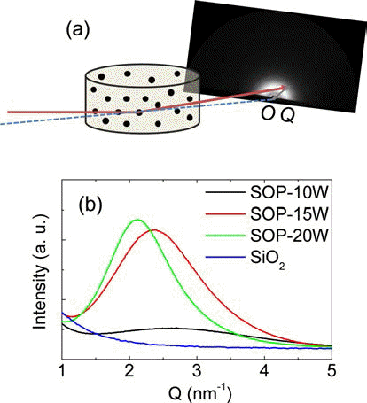
Fig. 5.
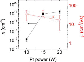
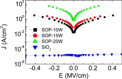
Fig. 7.

- 2-3 nm 크기의 Pt 나노분말이 균일하게 분산된 SiO2 복 합 박막을 코스퍼터링 방법으로 성장시켰다. Pt 타겟의 출 력을 10, 15, 20W로 조절함으로써 Pt 함량과 박막 성장 속도를 제어할 수 있었다. SPM과 TEM을 통해 박막의 표 면 거칠기와 미세 구조를 분석한 결과, Pt 나노분말의 크 기가 출력에 따라 점진적으로 증가하면서 rms 표면 거칠 기 또한 점차 증가했다. 특히 미세한 나노분말의 결정화 상태 역시 Pt 출력이 증가하면서 동반 증가했다. SAXS 분 석법을 통해 보다 넓은 영역에서 정교하게 나노분말의 형 상과 크기를 분석한 결과, SOP-10W, 15W, 20W에서 각각 약 2.3, 2.7, 3.0 nm 크기의 구형 나노분말이 형성된 것을 확인했고 이는 TEM 결과와도 잘 일치했다. SOP 복합막 의 전기 전도성을 분석해 본 결과, Pt 함량이 증가하면서 전기 전도성이 크게 향상 되는 것을 확인했다. 특히, Hall 효과에 의한 비저항과, capacitor 형태의 소자에서의 DC I-V 측정법에 의한 비저항이 큰 차이를 보였는데, 이는 Hall 효과 측정법에서 주입 또는 생성되는 단위 면적당 전자 농도가 크게 증가했기 때문인 것으로 생각 된다.
결 론
-
Acknowledgements
- 이 연구는 서울과학기술대학교 교내 학술연구비 지원으 로 수행되었습니다.
감사의 글
- 1. B Abeles, P Sheng, M.D Coutts and Y Arie: Adv. Phys., (1975) 24 407.Article
- 2. H.G Seo and S-T Oh: J. Kor. Powd. Met. Inst., (2014) 21 34.Article
- 3. G.E Jung and J.G Koh: J. Kor. Mag. Soc., (2005) 14 18.
- 4. T.H Kim, E.Y Jang, N. J Lee, D. J Choi, K.-J Lee, J Jang, J Choi, S. H Moon and J Cheon: Nano Lett., (2009) 9 2229.Article
- 5. S.C Ryu and J.Y Um: J. Kor. Cer. Soc., (2001) 38 412.
- 6. J-S Lee, J Cho, C Lee, I Kim, J Park, Y-M Kim, H Shin, J Lee and F Caruso: Nat. Nanotechnol., (2007) 2 790.ArticlePDF
- 7. S Choi, Y-K Cha, B-S Seo, S Park, J-H Park, S Shin, K.S Seol, J-B Park, Y-S Jung, Y Park, Y Park, I-K Yoo and S-H Choi: J. Phys. D., (2007) 40 1426.Article
- 8. D Lee and T.J Tseng: Appl. Phys., (2012) 110 114117.
- 9. C Chen, S Gao, G Tang, C Song, F Zeng and F Pan: IEEE Elec. Dev. Lett., (2012) 33 1711.Article
- 10. A Kanjilal, J.L Hansen, P Gaiduk, A.N Larsen, N Cherkashin, A Claverie, P Normand, E Kapelanakis, D Skarlatos and D Tsoukalas: Appl. Phys. Lett., (2003) 82 1212.ArticlePDF
- 11. J.G Perkins: J. Non-Cryst. Sol., (1972) 7 349.Article
- 12. B.A Van Hassel and A Burggraaf: ref title. J. Appl. Phys., (1989) 49 33.
- 13. B.J Choi, A.B.K Chen, X Yang and I-W Chen: Adv. Mater., (2011) 23 3847.Article
- 14. A.B.K Chen, S.G Kim, Y Wang, W-S Tung and I-W Chen: Nat. Nanotechnol., (2011) 6 237.ArticlePDF
- 15. T.C Chang, P.T Liu, S.T Yan and S.M Sze: Electrochem. Sol.-Stat. Lett., (2005) 8 G71.Article
- 16. Z Liu, C Lee, V Narayanan, G Pei and E.C Kan: IEEE Trans. Elec. Dev., (2002) 49 1606.Article
- 17. Z Liu, C Lee, V Narayanan, G Pei and E.C Kan: IEEE Trans. Elec. Dev., (2002) 49 1614.Article
- 18. J.H Yoon, J.H Han, J.S Jung, W Jeon, G.H Kim, S.J Song, J.Y Seok, K.J Yoon, M.H Lee and C.S Hwang: Adv. Mater., (2013) 25 1987.Article
- 19. J.R Levine, J.B Cohen, Y. W Chung and P Georgopoulos: J. Appl. Cryst., (1989) 22 528.Article
- 20. E Abrahams, P.W Anderson, D.C Licciardello and T.V Ramakrishnan: Phys. Rev. Lett., (1979) 42 673.Article
REFERENCES
Figure & Data
References
Citations
Citations to this article as recorded by 
 Cite this Article


Controlling Structural and Electrical Properties of Pt Nanopowder-Dispersed SiO2 Film


Fig. 1.
(a) Schematics of RF co-sputtering system with Pt and SiO2 target (off-axis), (b) variation in the thickness as a function of deposition time, where the slope of the linear fitting is considered as a growth rate of SOP and SiO2 films.
Fig. 2.
AFM image of (a) SiO2 27 nm, (b) SOP-10W 27 nm, (c) SOP-15W 22 nm, and (d) SOP-20W 22 nm. Rms roughness of the film was 0.69, 0.86, 0,97, and 1.22 nm, respectively.
Fig. 3.
Plan-view TEM image of (a) SOP-10W and (b) SOP- 20W film, respectively. Each inset figure is electron diffraction pattern.
Fig. 4.
(a) Schematics of SAXS analysis on SOP films, where incident beam is scattered by Pt nanopowders dispersed in SiO2 matrix. Scattering pattern represents the shape and size of the nanopowders. (b) SAXS spectra of SOP and SiO2 films, where the most probable size of the nanopowders were estimated to 2.33 (SOP-10W), 2.65 (SOP-15W), and 2.99 nm (SOP-20W).
Fig. 5.
Variation in the electron density, n (cm−3) and mobility, μ (cm2/Vs) of SOP films as a function of Pt power (i.e. Pt content).
Fig. 6.
J-E curves of SOP and SiO2 films in the low voltage region.
Fig. 7.
(a) Resistivity versus Pt power in the SOP and SiO2 films characterized by Hall effect and DC I-V measurements. (b) Schematics of the discrepancy between Hall effect and DC I-V measurements. Enhanced conductivity (σHall) by Hall effect measurement can be explained as a populated electron density in the film.
Fig. 1.
Fig. 2.
Fig. 3.
Fig. 4.
Fig. 5.
Fig. 6.
Fig. 7.
Controlling Structural and Electrical Properties of Pt Nanopowder-Dispersed SiO2 Film
| SiO2 | SOP-10W | SOP-15W | SOP-20W | |
|---|---|---|---|---|
| Growth rate (nm/min) | 1.66 | 2.17 | 2.70 | 3.24 |
| Pt content | 0 | 0.20 | 0.33 | 0.45 |
| Size of Pt nanopowders (nm) | 0 | 2.33 | 2.65 | 2.99 |
Table 1.
Growth rate, Pt content, and the size of Pt nanopowders in SOP and SiO2 films
Table 1.
TOP
