
Articles
- Page Path
- HOME > J Powder Mater > Volume 31(1); 2024 > Article
-
Review Paper
- Research Trends in Electromagnetic Shielding using MXene-based Composite Materials
- Siyeon Kima, Jongmin Byuna,b,*
-
Journal of Powder Materials 2024;31(1):57-76.
DOI: https://doi.org/10.4150/KPMI.2024.31.1.57
Published online: February 28, 2024
1Department of Materials Science and Engineering, Seoul National University of Science and Technology, Seoul 01811, Republic of Korea
2The Institute of Powder Technology, Seoul National University of Science and Technology, Seoul 01811, Republic of Korea
- *Corresponding Author: Jongmin Byun, Tel: +82-2-970-6619, FAX: +82-2-973-6657, Email: byun@seoultech.ac.kr
- - S. Kim 학생, J. Byun: 교수
• Received: January 25, 2024 • Accepted: February 8, 2024
© 2024 The Korean Powder Metallurgy & Materials Institute
This is an Open Access article distributed under the terms of the Creative Commons Attribution Non-Commercial License (http://creativecommons.org/licenses/by-nc/4.0/) which permits unrestricted non-commercial use, distribution, and reproduction in any medium, provided the original work is properly cited.
- 11,552 Views
- 186 Download
- 7 Crossref
Abstract
- Recent advancements in electronic devices and wireless communication technologies, particularly the rise of 5G, have raised concerns about the escalating electromagnetic pollution and its potential adverse impacts on human health and electronics. As a result, the demand for effective electromagnetic interference (EMI) shielding materials has grown significantly. Traditional materials face limitations in providing optimal solutions owing to inadequacy and low performance due to small thickness. MXene-based composite materials have emerged as promising candidates in this context owing to their exceptional electrical properties, high conductivity, and superior EMI shielding efficiency across a broad frequency range. This review examines the recent developments and advantages of MXene-based composite materials in EMI shielding applications, emphasizing their potential to address the challenges posed by electromagnetic pollution and to foster advancements in modern electronics systems and vital technologies.
- In recent years, the impact of electromagnetic radiation emitted from electronic devices such as mobile devices and wireless communication equipments on human health has surged, leading to the issue of electromagnetic pollution. This type of pollution may negatively affect the lifespan of electrical products and human health [1, 2]. Notably, the recent advancement in 5G communication technologies has introduced unprecedented levels of electromagnetic pollution. The pollution caused by electromagnetic waves is particularly critical in fields involving electromagnetic devices or radar systems. In the military sector, electromagnetic pollution poses a significant threat to vital aspects such as stealth capabilities and the stability of missile systems [3, 4]. Furthermore, when electric fields interfere with one another, distortion of electromagnetic signals may occur, leading to problems like impaired signal transmission and data loss. Therefore, with the rapid development of information technology and portable wearable devices, research into electromagnetic interference (EMI) shielding materials is imperative to address complex electromagnetic environments, ensure stable operation of equipment, and protect human health [5]. For practical application, EMI shielding materials must possess light weight, strong absorption strength, and an effective absorption band gap [6, 7]. Typically, dielectric loss materials such as electrically conductive metals or insulating polymers are used. These materials interact with electromagnetic fields, reflecting or absorbing electromagnetic waves, thereby reducing their amplitude and achieving a shielding effect. However, facing increasingly severe electromagnetic pollution, single materials often reach their limits due to the mismatch between dielectric and magnetic properties [8, 9]. Additionally, EMI shielding materials cannot block light or heat, which may limit the environments in which they can be used, and their effectiveness can be constrained if the material's thickness is less than the wavelength of the waves. To overcome these limitations, composite materials that can form multilayer structures without increasing weight or volume are required. Among various composite materials, those utilizing MXene stand out due to their excellent electrical properties and conductivity, offering superior shielding efficiency across a broad frequency range. Therefore, research into EMI shielding composite materials based on MXene is being actively pursued.
1. Introduction
- 2.1. MXenes
- MXenes are typically developed through the selective etching of the ‘A’ element from a layered MAX phase structure. Here, MAX is commonly denoted as Mn+1AXn (where n = 1, 2, or 3), with ‘M’ representing an early transition metal (such as Zr, Mo, Ti, Nb, etc.), ‘A’ indicating a group IIIA or VIA element (like Al and Si), and ‘X’ signifying carbon or nitrogen. MXenes are expressed as Mn+1XnTx (n = 1, 2, or 3), where ‘Tx’ stands for surface terminations such as -OH, -F, -O. Structurally, MXenes exhibit hydrophilicity and conductivity, and some display a certain degree of magnetism dependent on the 'M' element [10]. This unique combination of attributes can be further tuned by manipulating the composition and surface groups. MXenes are innovative two-dimensional materials with a large specific surface area and abundant surface functionalities. The layered structure and extensive specific surface area of MXene materials facilitate surface modification and electron transfer [11]. With excellent interlayer electronic coupling and conductivity, MXenes show remarkable electromagnetic absorption performance. This suggests the potential of MXenes to serve as effective two-dimensional materials for electromagnetic protection [12, 13].
- 2.2. Electromagnetic interference and microwave absorption
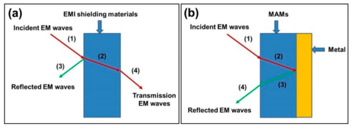
- Electromagnetic Interference (EMI) shielding and Microwave Absorbing (MA) represent two principal strategies to counteract the intrusion of incident electromagnetic waves, typically evaluated by distinct measurement models [15]. EMI shielding research is pertinent when electromagnetic waves are generated or could impact other devices. EMI shielding materials enhance the stability and reliability of electronic devices by minimizing electromagnetic interference through the blocking or reflection of electromagnetic waves. MA research is primarily utilized in the military and security sectors to advance electromagnetic wave technologies, for instance, in radar detection and recognition systems. These materials absorb electromagnetic waves, reducing or attenuating the wave velocity, thereby controlling the reflection, transmission, and absorption characteristics of the electromagnetic waves. Thus, both EMI shielding and MA research are considered critical technical requisites across various fields.
- Electromagnetic shielding is the ability of a shielding material to attenuate incident electromagnetic waves. This is denoted by the total shielding effectiveness (SET) or by the reflection loss (RL)/reflection coefficient (RC) [16].
- EMI shielding consists of reflection, absorption, and multiple reflection phenomena [17]. Sheketoff’s theory articulates the total shielding effectiveness (SET) as the sum of attenuations obtained from reflection (SER), absorption (SEA), and multiple reflections (SEM) [18, 19] :
- In the context of electromagnetic shielding, the attenuation due to multiple reflections is considered to be less significant compared to reflection and absorption. The shielding related to multiple reflections is directly associated with absorption, and it is generally accepted that multiple reflections can be neglected when the total shielding effectiveness (SET) is greater than or equal to 10 dB [20]. In the EMI shielding model (Figure 2a), the primary concern is the attenuation of the transmitted electromagnetic waves’ intensity, with shielding effectiveness (SE) being used as a common parameter to describe the relationship between transmitted and incident waves. In such cases, a high reflectivity is very advantageous for SE, with most of the incident waves being reflected at the surface of the shielding material. The physical importance of reflection loss in EMI shielding lies in the difference between the initial incident waves and the waves that penetrate the shielding material.
- Microwave Absorption (MA) is a phenomenon that occurs when electromagnetic waves interact with a material. Microwave electromagnetic waves, comprised of specific frequencies and amplitudes, spread into a material and interact with its molecules. This interaction results in the absorption of electromagnetic waves, leading to a reduction in their amplitude. The diminished electromagnetic waves can no longer pass through the object and are reflected or scattered instead. Additionally, as the microwaves are absorbed, the molecules or ions within the material vibrate, converting electrical energy into thermal energy, thereby raising the internal temperature of the material. In the MA model (Figure 2b), a metal substrate is arranged to reflect the transmitted waves. Consequently, the transmitted waves can always be disregarded in MA. Here, reflection loss refers to the difference between the initial incident waves and the final reflected waves [21].
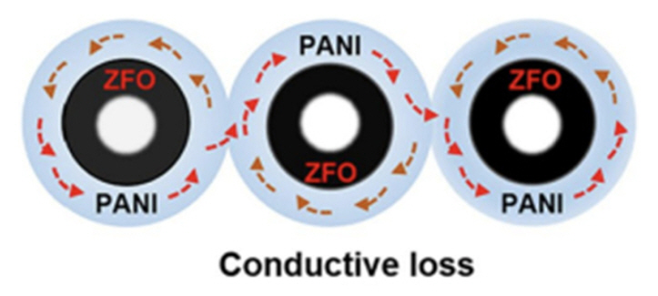
- The most common conductive absorptive materials are metals, which possess high conductivity. Conductive materials exhibit a conductive absorption mechanism. When Electromagnetic Waves (EMWs) impinge upon an absorptive material, as illustrated in Figure 3 an appropriate structure along with conductivity can result in multiple reflection effects, allowing the EMWs to be fully lost within the absorption layers [22]. Under the radiation of Electromagnetic Waves (EMWs), the principle of absorption in conductive absorptive materials is primarily based on the attenuation of EMW energy through electron movement and transition within the material itself. The influence of EMWs induces electromotive force, resulting in electron movement. When an electromotive force is present, directional movement of electrons occurs, causing the EMWs to incur ohmic losses and convert energy into heat. Electron transition, as a function of temperature, activates electrons at high temperatures, allowing them to overcome barriers and increase conductive loss. Metallic materials form current through the movement of free electrons, with some of the energy being converted into heat, resulting in losses in the presence of resistance. To maximize electromagnetic attenuation, the material must have sufficient conductivity and carrier mobility. However, high conductivity is not the sole criterion for substantial electromagnetic attenuation. This is because ‘connectivity’ is a prerequisite for achieving overall high conductivity in the conductive pathway [23]. Therefore, a specific conductive network must be formed to attain high conductivity [24, 25, 26].
- Dielectric loss is characterized by the electronic interactions between the electric field of incident Electromagnetic Waves (EMWs) and nanomaterials, leading to reflection loss. The capacity for dielectric loss primarily stems from electrical conductivity loss and polarization relaxation loss [28, 29]. Polarization relaxation loss is subdivided into ionic polarization, electronic polarization, dipolar relaxation polarization, and interfacial polarization [30]. Ionic polarization occurs due to the relative displacement of cations and anions. Electronic polarization happens with the positional change of constituent atoms relative to the atomic nucleus, thereby creating a dipolar moment. Ionic and electronic polarizations typically manifest in the frequency ranges of ultraviolet, visible, and infrared light, which are significantly higher than the microwave frequency range and are usually disregarded. Dipolar relaxation polarization refers to the polarization that occurs as dipolar moments rotate in alignment with the direction of the electric field. Relaxation loss can be analyzed through the Debby equation [31-33] :
- Here, εS represents the static permittivity, ε∞ is the permittivity at infinite frequency, and τ is the relaxation time. ε' is related to energy storage, while ε'' signifies energy loss. The equation of a circle formed using the above two equations is known as the Cole-Cole semicircle. The points on the semicircle correspond to the real and imaginary parts of the dielectric constant at specific frequencies calculated by the Debby equation. Interfacial polarization typically occurs at the interface of heterogeneous materials, where electrons or ions accumulate at the interface under the influence of an external electric field [34, 35].
- Magnetic loss refers to the phenomenon where external work on magnetic materials is converted into heat during the magnetization or demagnetization processes. This encompasses hysteresis loss, eddy current loss, and residual loss [36, 37]. Hysteresis loss arises from the hysteresis loop relationship between magnetic flux density and magnetic field strength [38, 39]. Eddy current loss occurs when a conductor moves within a non-uniform magnetic field or a time-varying magnetic field, which induces currents within the conductor itself.
- Here, δ denotes the electrical conductivity of the material, d is the thickness of the Microwave Absorbing Materials (MAMs), and f represents the frequency. μ' is related to energy storage, while μ'' signifies energy loss. From the above formula, C0 is a constant for a specific thickness of MAMs as the frequency changes. This is one of the methods used to determine if EMW loss occurs solely from eddy current losses. Residual loss refers to other losses excluding hysteresis and eddy current losses. Multi-loss materials are not merely simple single-loss mechanisms, but rather they combine the advantages of various types of losses [40].
- Electromagnetic shielding and absorption performance can be determined by the transmission line theory. The various electromagnetic parameters mentioned earlier are measured and derived according to the following differential equation.
- Here, ZO is the impedance of free space, Zin in is the input impedance of the absorber, f is the frequency of the microwaves, c is the speed of light, and d is the thickness of the absorber.
- According to equation (6), the impedance matching
2. Theoretical background
2.2.1. Electromagnetic interference and microwave absorption principles
2.2.2. Conductive loss
2.2.3. Dielectric loss
2.2.4. Magnetic loss
2.2.5. Electromagnetic wave shielding and absorption performance
- 3.1. Non-metallic material/MXene composite materials
- Ping Song et al. fabricated a honeycomb structure of reduced graphene oxide (rGH) to be used as a mold [43]. Through electrostatic adsorption, MXene self-assembled onto the rGH to form a honeycomb structure of rGO-MXene (rGMH). Subsequently, by synthesizing with epoxy, they produced an rGMH/epoxy nanocomposite materials and measured its electromagnetic shielding and absorption performance. Through Figure 4, it can be observed that the electrical conductivity and EMI SE of the nanocomposite are enhanced under adjustable conditions by utilizing rGMH and MXene. The rGMH/epoxy nanocomposite materials, with a honeycomb cell size of 0.5 mm and containing 1.2w t% rGO and 3.3 wt% MXene, exhibited optimal electrical conductivity and EMI SE values. The electrical conductivity was 387.1 S/m, and the EMI SE was around 55 dB. The paper reported an increase in electrical conductivity and EMI SE values with an increase in MXene content at a fixed honeycomb cell size. Additionally, it was found that the surface functionalities and defects of MXene contributed to the improvement of the EMI SE values by increasing space charge polarization in the alternating electromagnetic field. Moreover, the study compared absorption shielding effectiveness with reflection shielding effectiveness, finding a significantly higher proportion of absorption in the total shielding effectiveness, thereby establishing that the primary electromagnetic attenuation mechanism in rGMH/epoxy is absorption.
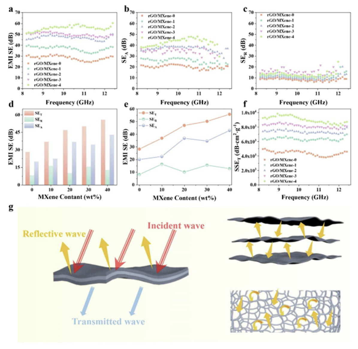
- Yu Zhang et al. employed a small amount of polyvinyl alcohol as an adhesive to apply rGO/MXene to spun laced nonwoven fabric using a dip-dry-reduction method, forming a composite film with a honeycomb cell-shaped sandwich structure [44]. The paper also observed a trend of increasing SET and specific EMI shielding performance (SSET) values with rising MXene content. The EMI SE value reached a considerable 60.42dB. This high value can be attributed to the enhanced electrical conductivity between the two-dimensional sheet layers. The composite material operates such that when EM waves encounter the film’s surface, a portion of the waves is reflected and absorbed, while the rest passes through, leading to multiple reflections and absorption between layers of rGO/MXene film. The schematic diagram presented in Figure 5 allows for confirmation of the described phenomenon. As the EM waves penetrate the middle layer, reflection and absorption occur amongst the conductive fibers, and the multiple reflections in the channels enhance the absorption of EM waves by the fibers covered with rGO/MXene nanosheets. Therefore, this paper also concludes that absorption loss predominates the electromagnetic attenuation mechanism.
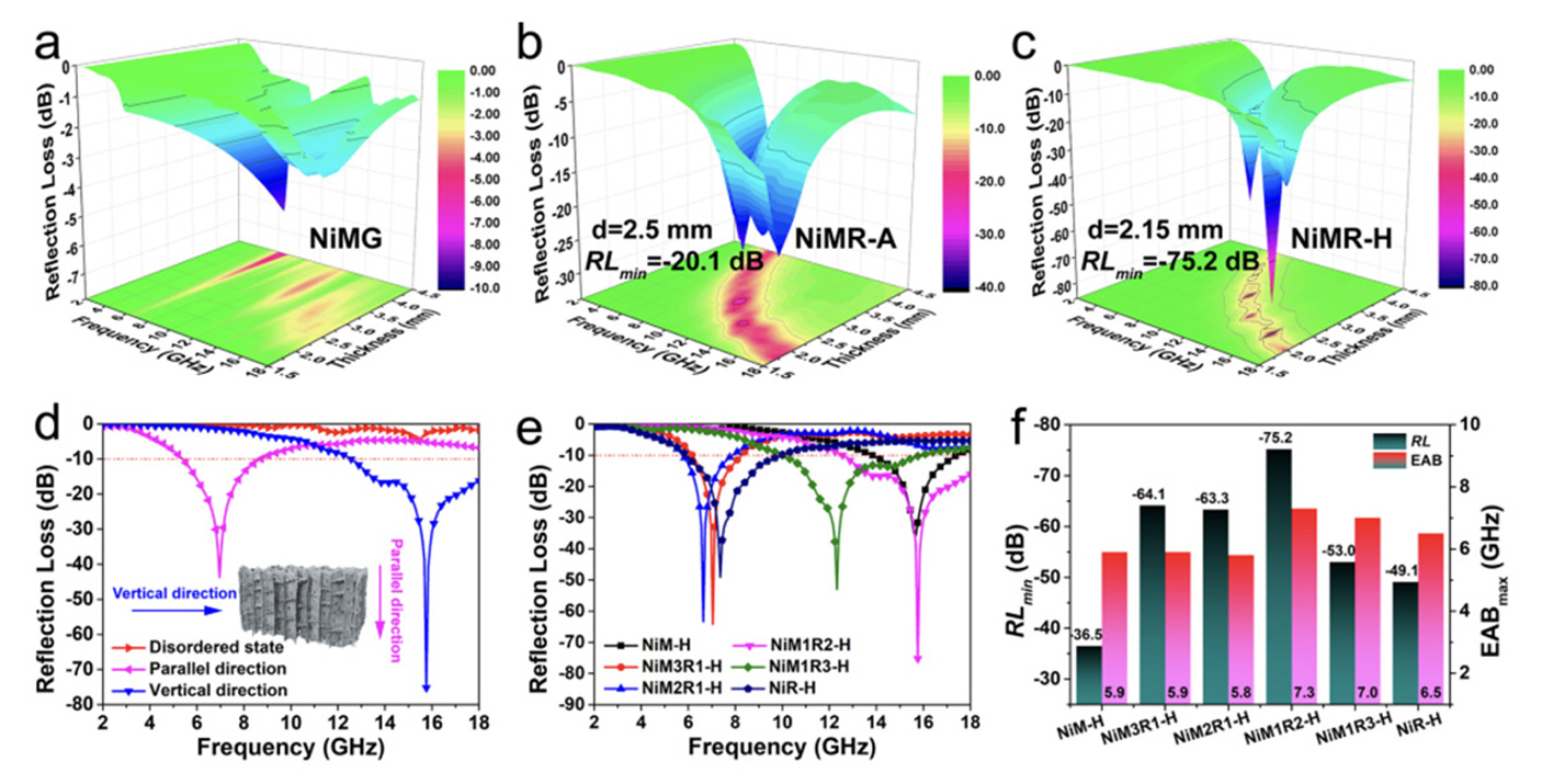
- Luyang Liang et al. developed an rGO/MXene aerogel [45]. This composite material recorded a minimum reflection loss (RLmin) value of -75 dB, signifying the ability to absorb 99.99996% of the waves. Additionally, the Effective Absorption Bandwidth (EAB) was measured at 7.3 GHz. Remarkably, these 3D dielectric/magnetic aerogels, featuring cell-unit structures oriented and supported by Ni nano chains, were prepared via a universal ice template method coupled with hydrazine vapor treatment. Compared to commercial polymer foams, they exhibit superior thermal insulation performance, making them suitable for applications in aerospace, stealth weaponry, and electromagnetic protection. Uniquely, the majority of the electromagnetic attenuation mechanism in the rGO/MXene aerogel was found to be reflective. Also, increasing the MXene to rGO ratio led to decreased polarization and conductive losses due to the progressively enhanced conductivity. The paper also tested the variance in EMA performance based on orientation. Disordered samples with irregular cell walls and disrupted networks failed to achieve sufficient polarization and continuous electronic conduction paths, resulting in very low EMA performance. However, in oriented composite materials, the reaction of the EMWs with the framework’s defects and functional groups resulted in strong dipolar polarization and multiple hetero-interface polarizations, significantly elevating the EMA performance.
- Comparison of EMA performances for Figure 6 (a), (d) a NiMR-H aerogel in the parallel direction, vertical direction, and disordered state and Figure 6 (e) NiMR-H aerogels with different MXene to GO ratios (NiM-H, NiM3R1-H, NiM2R1-H, NiM1R2-H, NiM1R3-H, and NiR-H correspond to ratios of 1:0, 3:1, 2:1, 1:2, 1:3, and 0:1, respectively). Figure 6 (f) Statistics of RLmin and EABmax for different NiMR-H aerogels [45].
- Tianqi Hou et al. used a small amount of polyvinyl alcohol as an adhesive to apply rGO/MXene to spun laced nonwoven fabric by a dip-dry-reduction method, forming a sandwich-structured composite film [46]. They then fabricated a NiCo/TiC/TiO/CNT film to measure its EMI shielding and absorption performance. The composite material exhibited remarkable broadband absorption properties, with a strong absorption value of -51.98 dB at 1.9 mm and a wide absorption bandwidth of 7.76 GHz at 2.1 mm. Compared to pure Ti3C2Tx MXene, it displayed notable improvements in RLmin and maximizing EAB. These enhancements are attributed to the laminar structure and the synergistic effects of polarization and magnetic losses. The composite material, composed of a spider-web-like interface layer of magnetic CNTs and MXene sheets, increased the EMW transmission path and facilitated the hopping electron pattern between adjacent carbon nanotubes, optimizing the impedance characteristics [47]. Furthermore, the magnetic phase of the magnetic CNTs within the composite materials enhanced magnetic loss, promoting actions such as natural resonance, exchange resonance, and eddy current loss, thereby balancing dielectric and magnetic losses and ensuring additional consumption of EMWs. They are presented in Figure 7.
- Zhiming Deng et al., in comparison to conventional MXene-aerogels, fabricated CNT-reinforced MXene-aerogel [48]. The MXene/CNT aerogels are reported to exhibit superelasticity, enhanced fatigue resistance, and high electrical conductivity. As shown in figure 8, the paper also noted an increase in EMI SE values with a rise in MXene content. Moreover, the porous structure of the Aerogels facilitated scattering and expanded the propagation path of the electromagnetic waves, promoting attenuation of EM energy within the MCA [49-51]. Such MCAs possess superior insulation capabilities compared to commercial MF and EPS foams and maintain excellent elasticity at high temperatures up to 300°C and at cryogenic temperatures in liquid nitrogen. The paper reported these characteristics as making anisotropic aerogels promising for electromagnetic protection applications.
- Meng Zhu et al. used bleached wood as an anisotropic framework for assembling with highly conductive f-Ti3C2 through hydrogen bonding [52]. The MXene and Wood (M@W) nanocomposite aerogels were obtained using a simple immersion and freeze-drying method. This anisotropic microstructure provides excellent EMI shielding performance due to tunnel-like electromagnetic pathways in the parallel growth direction. The EMI SE exhibited a high value of up to 72dB. As shown in Figure 9 the anisotropic structure of the wood skeleton leads to a layered microstructure, contributing to discontinuous conduction paths and ultra-low conductivity in the vertical growth direction, thereby enhancing electromagnetic absorption performance. When electromagnetic waves enter the M@W aerogel, their energy is converted into thermal energy through polarization relaxation and conductive loss [53]. The extensive barriers cause multiple reflections and scattering, significantly improving the dispersion of electromagnetic waves.
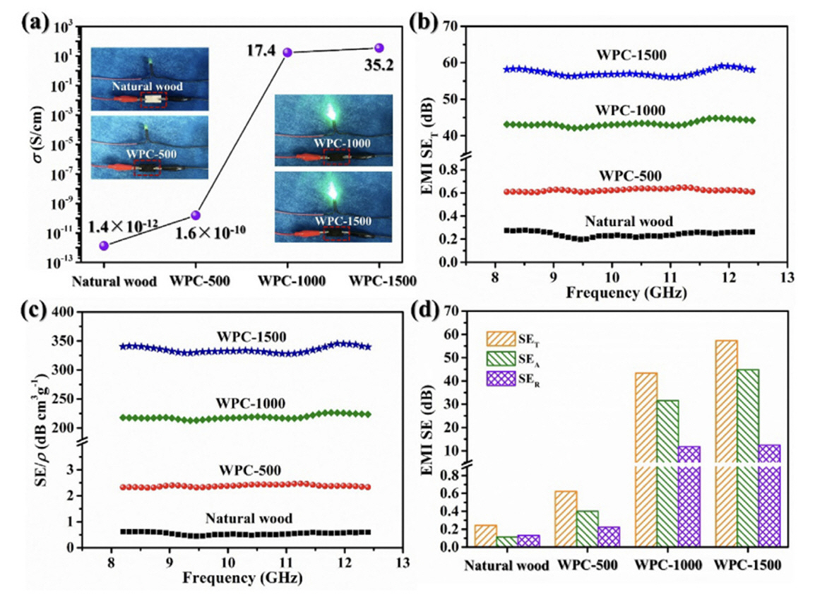
- Chaobin Liang et al. utilized a wood-derived porous carbon (WPC) skeleton, extracted from natural wood, as a mold. As shown in Figure 10, they fabricated an MXene aerogel/WPC composite materials by mixing the 3D MXene aerogel within high-purity honeycomb cells of WPC, using it as a microreactor [54]. The EMI SE measured at 71.3 dB, not only effectively addresses the instability issues of the MXene aerogel network but also significantly extends the transmission path of electromagnetic waves, converting incident waves into heat and electrical energy, thus delivering excellent EMI shielding performance. The composite materials also demonstrated superior anisotropic compressive strength, as well as excellent thermal insulation and flame retardancy. Such ultralight, green, and efficient multifunctional bio-carbonbased composite materials hold great potential for applications in advanced EMI shielding areas such as aerospace and defense industries.
- 3.2. Metallic materials/MXene composite materials
- Mixing magnetic metals with MXene not only imparts magnetism to the MXene itself but can also enhance electrical properties, mechanical strength, and thermal stability. Consequently, the effectiveness of electromagnetic shielding can also be increased.
- Tianqi Hou et al. enhanced the electromagnetic shielding effect by removing the Al layer from the MAX phase using hydrofluoric acid and allowing cobalt nitrate to react with TAA in solution through a hydrothermal reaction, followed by a heat treatment that transformed cobalt sulfide into Co9S8 nanoparticles [55]. As evident in Figure 11, composite materials with MXene contents of 100 g and 150 g exhibited good electromagnetic shielding effects. The team ensured that when electromagnetic waves impinged on the sample’s surface, the hybrid material's favorable impedance matching function allowed the waves to penetrate internally more easily instead of causing excessive reflection at the surface. As shown in Figure 12, the multicomponent form created numerous interfaces between Ti3C2TX, Co9S8, and C, which improved the conductive loss capability and formed interfacial polarization, thereby enhancing the dielectric loss capacity [56, 57]. In parallel, the introduction of Co9S8 particles and carbon sheets allowed the aggregation of charges at the uneven interfaces, aligning unique dipolar moments along the direction of the electric field and generating dipolar polarization [58]. Additionally, the unique accordion structure of the hybrid material induced multiple reflections and consumed multiple incident electromagnetic waves [59]. These factors worked together to improve the electromagnetic absorption performance of the hybrid material in all directions.
- Xiao Li et al. used a hydrothermal process to manufacture magnetic nanoplate and nanoflower-shaped FeCo powders and then formed an MXene/FeCo composite film through filtration [60]. Their study revealed that the nanoflower form exhibited superior magnetic properties and, consequently, better electromagnetic shielding effects than the nanoplate form. While the incorporation of FeCo disrupted the layered structure of MXene, as shown in Figure 13, reducing dielectric loss capability, it enhanced the magnetic loss capability, increasing the overall electromagnetic shielding effect. Typically, randomly distributed magnetic nanoparticles tend to aggregate due to their inherent magnetic attraction [61], which can cloak many magnetic surfaces, preventing them from fully exhibiting their magnetic properties and causing a serious imbalance in local matching that reduces electromagnetic attenuation. However, the team effectively dispersed FeCo nanoparticles using electrostatic magnetic self-assembly. The MXene nanosheets, being non-magnetic insulators, could effectively separate the nanoparticles, thus exposing more magnetic surfaces. As illustrated in Figure 14, the magnetic FeCo alloys between adjacent layers could interact through the ultra-thin MXene nanosheets, maintaining the film’s magnetic loss behavior. In the case of single FeCo alloy nanoflowers, they exhibit strong intrinsic magnetic signals with many flux lines, and the numerous irregular bumps on the FeCo alloy surface significantly enhance the flux line signals when they are grouped together. Unlike FeCo nanoplates, the magnetic coupling behavior in nanoflowers led to increased electromagnetic shielding effects. Additionally, the unique accordion structure of MXene played a vital role in enhancing the MA attenuation capability. The construction of a continuous conductive network using 2D MXene nanosheets provided multiple channels for carrier movement and hopping. Under the applied electric field, favorable conductive currents could be formed, converting the energy of incident electromagnetic waves into heat. Moreover, the special multilayer structure provided a large active area for multiple reflections and scattering of incident electromagnetic waves. Furthermore, both reduced dielectric constant and increased permeability were advantageous for proper impedance matching conditions, a prerequisite for extinguishing incident microwaves.
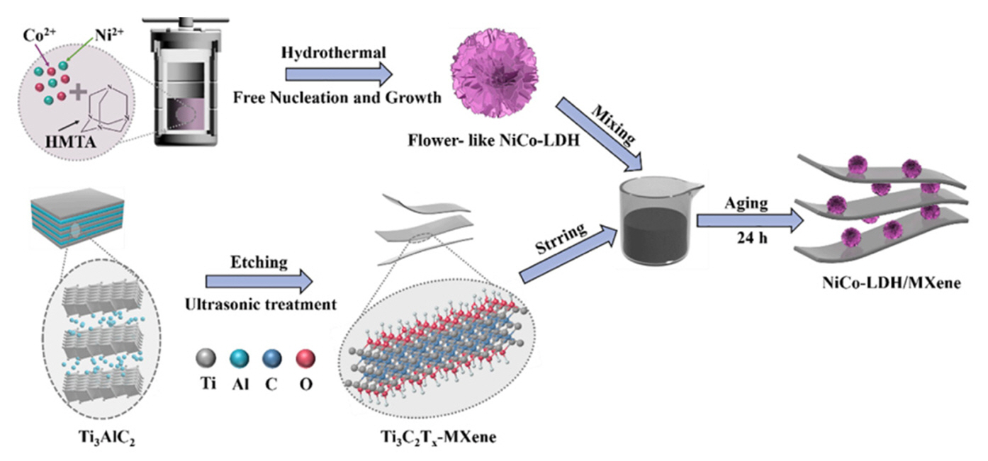
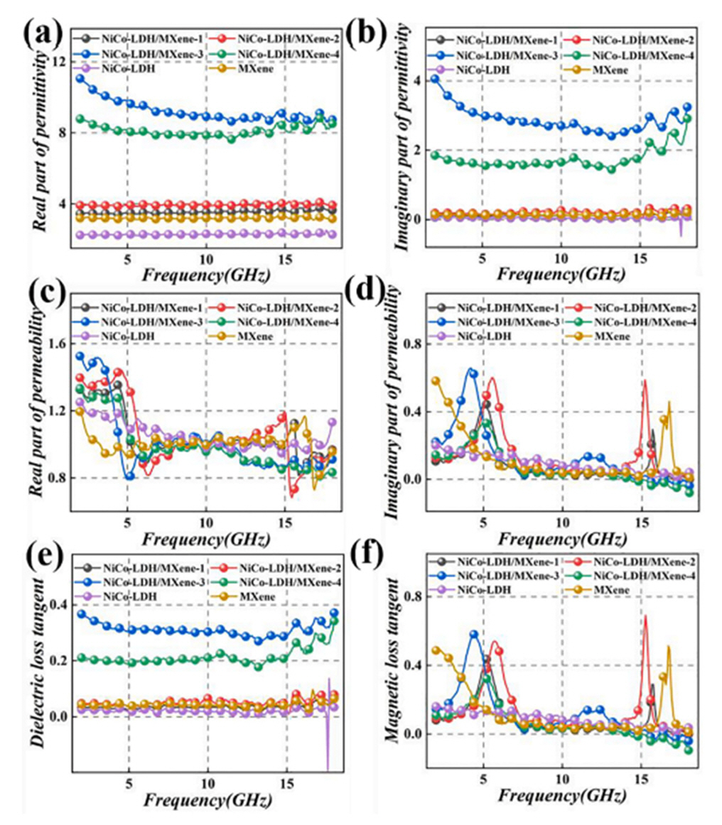
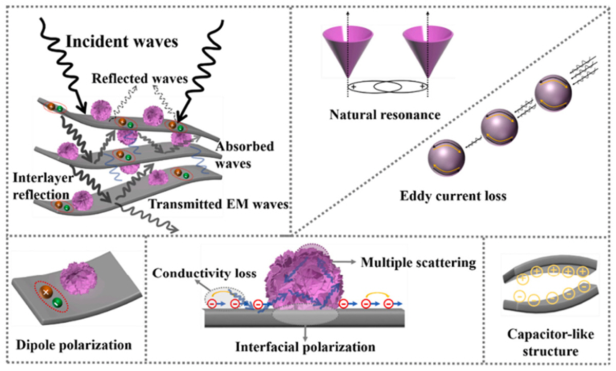
- Xuran Gao et al. utilized hydrofluoric acid to remove the Al layer, followed by ultrasonic treatment to produce MXene nanosheets [62]. Subsequently, flower-like NiCo-LDH was synthesized through a hydrothermal reaction of equal molar ratios of nickel nitrate hexahydrate and cobalt nitrate hexahydrate. As illustrated in Figure 15, the resulting MXene nanosheets and flower-like NiCo-LDH were mixed via a stirring process to fabricate the NiCo-LDH/MXene composite materials. As shown in Figure 16, it was commonly observed that as the MXene content increased, both the dielectric loss capability and the magnetic loss capability were enhanced, leading to better electromagnetic shielding effectiveness. However, the NiCo-LDH/MXene-4 sample (LDG:MXene =1:4) sample, with the highest MXene content, generally showed lower values than the NiCo-LDH/MXene-3 (LDH:MXene=1:3), indicating that the appropriate regulation of MXene content can aid in improving the dielectric properties of the hybrid. The unique structure derived from the flower-like NiCo-LDH and MXene nanoflakes provided the hybrid with abundant heterojunction interfaces, promoting multiple reflections and scattering of EMWs, effectively enhancing EMW extinction [63-65]. Moreover, as shown in Figure 17, the large surface area and high carrier density of the MXene nanoflakes satisfied the conditions for free electron transitions, and the conductive losses generated by electrons during transmission also contributed to EMW attenuation [66, 67]. Additionally, the ability to form micro-capacitor structures between MXene layers increased the dielectric loss capability.
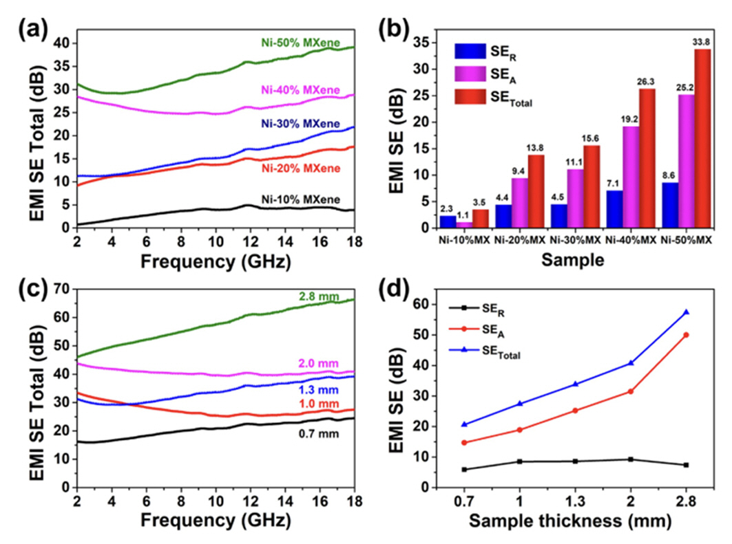
- Luyang Liang et al. utilized a hydrothermal process to mix Ni chains with Ti3C2Tx nanosheets, fabricating a Ti3C2Tx MXene/Ni chain hybrid [34]. That nanosheets can made as illustrated in Figure 18. When the MXene content reached 50 wt%, the EM SE attained 66.4 dB, with SEA accounting for 59.9 dB of the majority of the EM SE, as reported. They were also able to control the electromagnetic absorption and shielding characteristics by adjusting the MXene content. The 1D magnetic nano chains, resembling the structure of antennas, were able to receive more electromagnetic waves, inducing directional polarization attenuation and forming dissipated micro currents to absorb electromagnetic energy [68]. Under the influence of alternating electromagnetic waves, Ni chains could exhibit magnetic loss effects induced by natural resonance, exchange resonance, and eddy currents. Furthermore, the Tx sheets, acting as polarization centers in the electromagnetic waveband, could induce space charge polarization and interfacial polarization due to the accumulation of space charges at the interfaces between MXene sheet/Ni chain, MXene sheet/paraffin, and Ni chain/paraffin [69].
- Yuhong Cui et al. As shown in Figure 19, successfully fabricated rGO/MXene/Fe3O4 microspheres (FMCM) quickly and simply through an ultrasonic spray self-assembly method [70]. The electromagnetic wave loss of FMCM is primarily dielectric loss, accompanied by magnetic loss in the form of eddy current loss and natural resonance. FMCM, being porous with a high specific surface area, facilitates the entry of electromagnetic waves, thereby increasing electromagnetic loss, as reported. Additionally, an increase in pore size was noted to aid the entry of electromagnetic waves, improving the probability of electromagnetic wave reflective loss within the material’s pores. The residual surface oxygen functional groups, local defects, and charge carriers Tx of rGO and Ti3C2, under the influence of an electric field, could create dipoles to achieve dipolar polarization. Furthermore, the formation of a 3D conductive network effectively promoted the rapid transmission of free carriers, increasing conductive loss.
- Lei Cai et al. fabricated N-doped MXene (Ti3CNTx) flakes and hollow Co-ZIF (HCF) particles utilizing a controllable directional etching strategy and electrostatic self-assembly technology [71]. As shown in Figure 20, the hybrid’s electromagnetic wave absorption capability at 15.68 GHz with a thickness of 1.43 mm was reported to be -55.02d B. The hollow structure, endowed by directional etching, enhanced the reflection loss and magnetic loss capabilities of HCF. The open-wall structure of HCF, uniformly distributed on Ti3CNTx sheets, improved EMW extinction efficiency and impedance matching absorption function. Below the transmission threshold, the sample was dispersed in paraffin to form a conductive network. More electrons hopping between different layers and increased network conductivity converted more EMW energy into thermal energy. Additionally, the HCF was electrostatically mounted onto Ti3CNTx sheets, eliminating aggregation issues and improving magnetic loss. The introduction of magnetic HCF also improved the hybrid’s dielectric constant, enhancing impedance matching at high attenuation factors and ensuring smooth entry of EMWs as absorbers. Thus, the paper reported the potential of this hybrid as a high-performance EMW absorbing material.
- Ying-jie He et al. manufactured a multifunctional PCM composite materials by encapsulating polyethylene glycol (PEG) into a porous MXene/silver nanowire (AgNM) hybrid sponge via vacuum impregnation [72]. As shown in Figure 21, The EMI SE was reported to range from 12.3 to 30.5 dB, and by integrating shape memory functionality into the composite materials, they achieved adjustable EMI shielding performance. The large porous framework of the MF@MA/PEG composite materials, along with excellent electrical conductivity, impedance matching of microwaves, and multiple reflections, allowed for high EMI SE. As the composite material was compressed, the surrounding MA fillers formed closer contacts, creating more complete conductive paths, which would enhance impedance mismatch and the degree of microwave reflection. However, a decrease in micro-wave absorption occurred under compression. This was due to a significant reduction in internal multiple reflections caused by cell closure, which could surpass the improved reflective loss derived from compact MA connections [73].
- Wei Chen et al. demonstrated a vacuum-assisted layer-by-layer assembly technique for uniformly depositing electrically conductive materials on fibers to develop multifunctional and flexible fibers [74]. Consequently, highly conductive veins were created using nanomaterials composed of silver nanowires (AgNWs) and laminar structured transition metal carbides/nitrides (MXene) nanosheets. The EMI SE was reported to be 54 dB, indicating high EMI shielding efficiency, and the team was successful in manufacturing a transparent and conductive film with high light transmittance. The MXene coating adhered and activated the joints of the AgNW network, effectively enhancing the interconnectivity and integrity with the activated PET substrate. Compared to neat AgNW films with the same AgNW loading, the MXene-integrated AgNW films exhibited much higher shielding performance and improved mechanical and environmental stability. Additionally, the macroscopic scale hierarchical structure design ensured much higher EMI shielding performance with a high light transmittance of ~83%. The report indicated that such multi-layer structure optimization strategies could be applied to the fabrication of other high-performance transparent and conductive EMI shielding materials. The information provided in Figure 22 for further elucidation.
3. Research trends in electromagnetic wave shielding/absorption of MXene-based composite materials
3.1.1. Carbon nanomaterial/MXene composite materials
3.1.1.1. reduced graphine oxide (rGO)/MXene composite materials
3.1.1.2. Carbon Nano Tubes(CNTs)/MXene composite materials
3.1.1.3. Wood/MXene composite materials
3.2.1. Magnetic metal material/MXene composite materials
3.2.1.1. Magnetic metal/MXene composite materials
3.2.1.2. Magnetic metal oxide/MXene composite materials
3.2.2. Metallic material/MXene composite materials
- In modern society, electromagnetic waves are generated through various electronic devices such as wireless communications, television, and mobile phones, and are also propagated through infrastructure like power lines, wireless internet, and satellite communications. While these devices provide convenience and innovation in our daily lives, they can also pose problems related to electromagnetic wave exposure. Therefore, research into electromagnetic shielding is essential to create a safe and stable environment unaffected by electromagnetic waves, contributing to the sustainable development and qualitative improvement of contemporary society. Hence, electromagnetic shielding research necessitates ongoing attention and investment for our safety and convenience. MXenes can be significantly beneficial in such research. Due to their excellent conductivity, they can effectively contribute to the absorption and reflection of electromagnetic waves and are versatile enough to address a wide frequency band, making them suitable for use as electromagnetic shielding materials across various frequency ranges. Consequently, research into electromagnetic shielding using MXenes is receiving considerable interest. Various researchers are exploring the electromagnetic shielding characteristics and potential applications of MXenes, with their importance growing as communication technologies like 5G evolve. Future research should therefore focus on enhancing electromagnetic shielding performance through the combination of MXenes with other materials and expanding their adaptability across a more extensive range of frequency bands.
4. Conclusion
-
Acknowledgements
- This work was supported by the National Research Foundation of Korea (NRF) grant funded by the Korean government (Ministry of Science and ICT) (NRF2021 R1F1A1061792)
Fig. 1.A periodic table color-coded to indicate the composition of MXenes and a classic diagram of the MXene structure [14].


Fig. 4.σ (a–c) and EMI SET (a'–c') values of the rGMH/epoxy nanocomposite materials with different cell sizes; σ (d) of the rGMH-5 (MXene 90g/L including) nanocomposite materials at different directions; σ (e) and EMI SET (e') values of the rGM/epoxy nanocomposite materials [43].
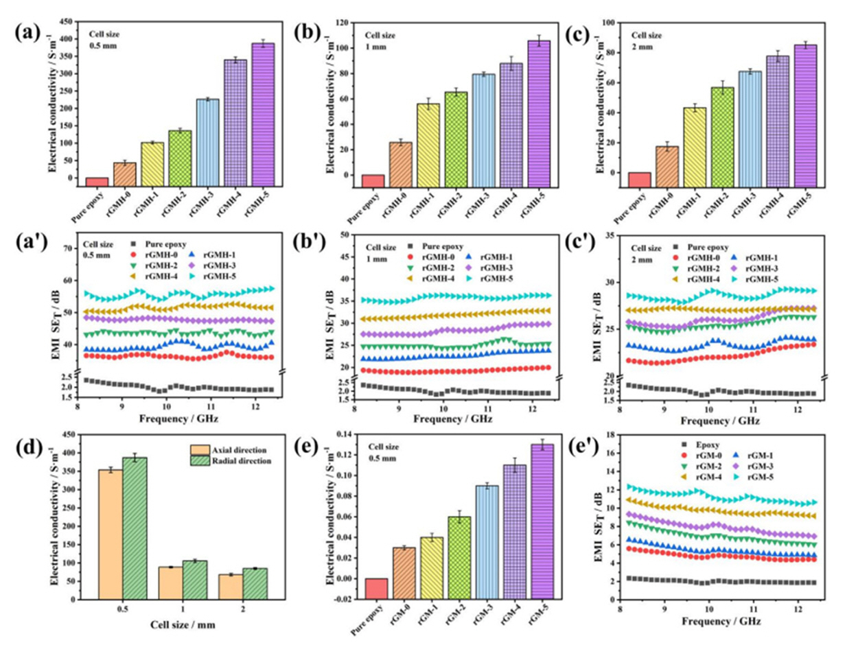
Fig. 5.(a) SET, (b) SEA, (c) SER of rGO/MXene-x. (d) and (e) The average EMI SE of rGO/MXene-x. (f) The SSET of rGO/MXene-x. (g) Electromagnetic shielding mechanism diagram of rGO/MXene-x [44].

Fig. 6.Three-dimensional RL–f curves of (a) NiMG, (b) NiMR-A, and (c) NiMR-H aerogels. Comparison of EMA performances for (d) a NiMR-H aerogel in the parallel direction, vertical direction, and disordered state and (e) NiMR-H aerogels with different MXene to GO ratios (NiM-H, NiM3R1-H, NiM2R1-H, NiM1R2-H, NiM1R3-H, and NiR-H correspond to ratios of 1:0, 3:1, 2:1, 1:2, 1:3, and 0:1, respectively). (f) Statistics of RLmin and EABmax for different NiMR-H aerogels [45].

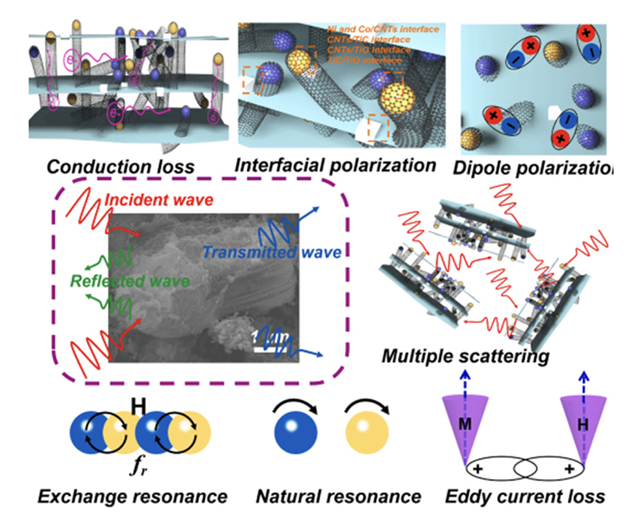
Fig. 8.(a) Plots of electrical conductivity vs MXene content for MCAs. (b) Resistance change rates of MCA-1 during compression cycles at different strains. (c) Plots of EMI shielding effectiveness of MCAs. (d) EMI shielding performances of MCA-1 with different densities at the thickness of 2 mm. (e) Comparison of EMI shielding performances of MCA (red stars) and those of EMI shielding nanomaterials reported in the literature. (f) Schematic of EMI shielding mechanisms of MCA [48].

Fig. 9.(a) Electrical conductivities of the M@W nanocomposite aerogel, (b) EMI shielding efficiencies of the M@W nanocomposite aerogel, (c) average EMI shielding effectiveness of the M@W nanocomposite aerogel, (d) EMI SE/r of the M@W nanocomposite aerogel c, (e) the comparison of M@W nanocomposite aerogel with other reported materials, and (f) the proposed illustration of the shielding mechanism for the M@W nanocomposite aerogel at parallel growth direction [52].

Fig. 10.(a) r, (b) EMI SET, (c) SE/q and (d) SEA & SER of natural wood, WPC-500, WPC-1000 and WPC-1500 (WPC-carbonization degree) [54].

Fig. 11.Frequency dependence of (a) ε', (b) ε'', (c) μ', (d) μ'', (e) Tanδε, and (f) Tanδμ of Ti3C2Tx, Co9S8/C, Co9S8/C/Ti3C2Tx-50, Co9S8/C/Ti3C2Tx-100 and Co9S8/C/Ti3C2Tx-150 [55].
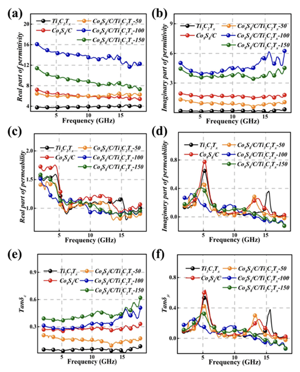
Fig. 12.Schematic illustration of the possible electromagnetic absorption mechanism of Co9S8/C/Ti3C2Tx-100 [55].
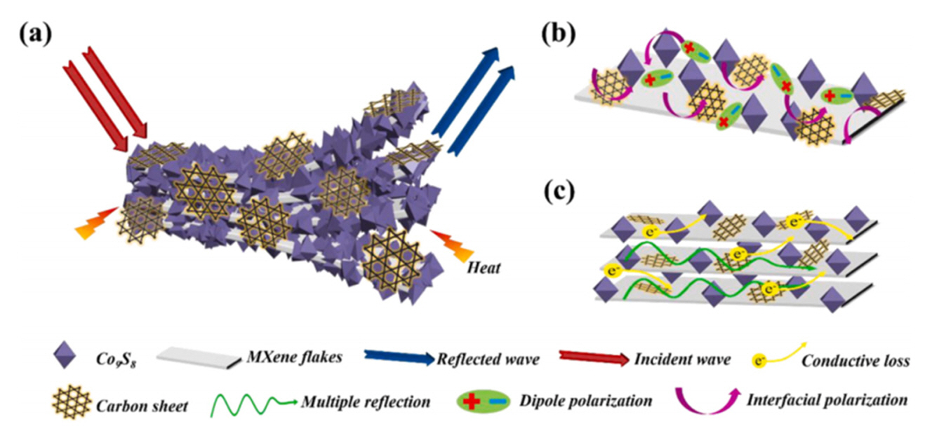
Fig. 13.Electromagnetic parameters of pure MXene film, MFC-1 (MXene and nanoplate like FeCo) and MFC-2 (MXene and nanoflower like FeCo) samples: (a) real and (b) imaginary part of complex permittivity, (c) dielectric loss tangent, (d) real and (e) imaginary part of complex permeability, and (f) magnetic loss tangent [60].

Fig. 14.(a, e) TEM images, (b, f) off-axis electron holograms, (c, g) magnetic flux lines and (d, h) schematic illustration of nanoflower-like FeCo alloy; (i) schematic illustration of MFC-2 [60].
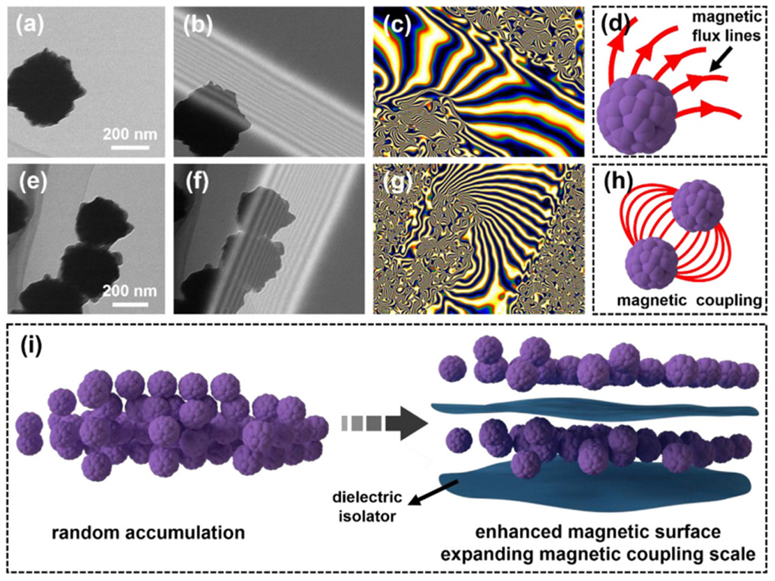

Fig. 16.real part (a) and imaginary part (b) of complex permittivity of the six samples; real part (c) and imaginary part (d) of complex permeability of the six samples; dielectric loss tangent (e) and magnetic loss tangent (f) of the six samples [62].


Fig. 18.(a) Shielding performance of MXene/Ni hybrids with different Ti3C2Tx contents ranging from 10 to 50wt % and (b) the corresponding average value of SEtotal, SEA, and SER of 2–18GHz, (c) the SEtotal curve of Ni-50% MXene with different thicknesses, and (d) the corresponding average value of SEtotal, SEA, and SER [34].


Fig. 20.3D RL and contour map of the samples with different thicknesses (1.0–5.0mm) from 2.0 to 18.0GHz: Ti3CNTx (a, b), Ti3CNTx/HCF hybrids (d, e) and HCF (g, h); RLmin for Ti3CNTx, Ti3CNTx/HCF hybrids and HCF (c); the quarter wavelength thickness matching of Ti3CNTx/HCF hybrids (f, i) [71].

Fig. 21.(a) Sheet resistances and (b) EMI shielding performances of (MAX)n silk textile with different spray cycles and concentrations. (c) Plots of EMI SE versus spray cycles for (MA0.8)n silk textile. (d) Synergistic effect of AgNW and MXene on the EMI SE and the sheet resistances of functional silk textiles. (e) EMI shielding performances of (MA1)10 silk textile with different thicknesses. (f) EMI shielding performances and sheet resistances of (MA1)10 textiles with different textile substrate (silk, cotton, nylon, and wool) [72].

Fig. 22.(a) Schematic illustration of the preparation process of the d-MA film. Inset is a close-up photo of the d-MA film. (b) EMI shielding performances of AgNW, MA2m/2n, and d0.2-MAm/n films at various AgNW densities. Both MA2m/2n and dx-MAm/n films possess the same loading density. (c) Transmittances of MA films with different AgNW densities. (d) Relative transmittances of MA20/164 and d-MA10/82 films with various gap distances. (e) EMI shielding performances of MA films with various gap distances. (f) Experimental and simulated SE values for MA and d-MA films with various gap distances. (g) Schematic of the EMI shielding mechanisms of a d-MA film [74].

- 1. J. W. Li, Y. Q. Ding, Q. Gao, H. M. Zhang, X. H. He, Z. L. Ma, B. Wang and G. C. Zhang: Compos. B Eng., 190 (2020) 107935.Article
- 2. G. H. Wang, L. L. Hao, X. D. Zhang, S. J. Tan, M. Zhou, W. H. Gu and G. B. Ji: J. Colloid Interface Sci., 607 (2020) 89.Article
- 3. X. Zhou, Z. Jia, X. Zhang, B. Wang, W. Wu, X. Liu, B. Xu and G. Wu: J. Mater. Sci. Technol., 87 (2021) 120.Article
- 4. J. Cheng, H. Zhang, Y. Xiong, L. Gao, B. O. Wen, H. Raza, H. Wang, G. Zheng and D. Zhang: J. Materiomics., 7 (2021) 1233.Article
- 5. H. Y. Wang, X. B. Sun, S. H. Yang, P. Y. Zhao, X. J. Zhang, G. S. Wang and Y. Huang: Nano-Micro Lett., 13 (2021) 1.
- 6. B. W. Deng, Z. Xiang, J. Xiong, Z. C. Liu, L. Z. Yu and W. Lu: Nano-Micro Lett., 12 (2020) 55.
- 7. X. F. Zhou, Z. R. Jia, A. L. Feng, K. K. Wang, X. H. Liu, L. Chen, H. J. Cao and G. L. Wu: Compos. Commun., 21 (2020) 100404.Article
- 8. C. Zhang, W. K. Cao, L. T. Wu, J. C. Ke, Y. Jing, T. J. Cui and Q. Cheng: Appl. Phys. Lett., 118 (2021) 133502.
- 9. C. X. Wang, B. B. Wang, X. Cao, J. W. Zhao, L. Chen, L. Chen, L. Shan, H. Wang and G. Wu: Compos. Part B Eng., 205 (2021) 108529.Article
- 10. M. Khazaei, M. Arai, T. Sasaki, C-Y. Chung, N.S. Venkataramanan, M. Estili, Y. Sakka and Y. Kawazoe: Adv. Funct. Mater., 23 (2013) 2185.Article
- 11. F. Wang, N. Wang, X. Han, D. Liu, Y. Wang, L. Cui, P. Xu and Y. Du: Carbon., 145 (2019) 701.Article
- 12. Y. Guo, D. Wang, T. Bai, H. Liu, Y. Zheng, C. Liu and C. Shen: Adv. Compos. Hybrid Mater., 4 (2021) 602.ArticlePDF
- 13. H. Cheng, Y. Pan, Q. Chen, R. Che, G. Zheng, C. Liu, C. Shen and X. Liu: Adv. Compos. Hybrid Mater., 4 (2021) 505.ArticlePDF
- 14. Y. Gogotsi and Q. Huang: ACS Nano., 15 (2021) 5775.Article
- 15. J. H. Burroughes, D. D. C. Bradley, A. R. Brown, R. N. Marks, K. Mackay, R. H. Friend, P. L. Burns and A. B. Holmes: Nature., 347 (1990) 539.ArticlePDF
- 16. X. Yin, L. Kong, L. Zhang, L. Cheng, N. Travitzky and P. Greil: Int. Mater. Rev., 59 (2014) 326.Article
- 17. Y. Cheng, H. Zhao, H. Lv, T. Shi, G. Ji and Y. Hou: Adv. Electron. Mater., 6 (2020) 1900796.
- 18. S. A. Schelkunoff: Electromagnetic Waves, Bell Telephone Laboratories Series., (1943.
- 19. R. B. Schulz, V. C. Plantz and D. R. Brush: IEEE Trans. Electromagn. Compat., 30 (1988) 187.Article
- 20. H. Wang, Z. Zhang, C. Dong, G. Chen, Y. Wang and H. Guan: Sci. Rep., 7 (2017) 15841.
- 21. Y. Wang, Y. Du, P. Xu, R. Qiang and X. Han: Polymers (Basel)., 9 (2017) 29.Article
- 22. X. Han and Y. S. Wang: Phys. Scr., 129 (2017) 335.
- 23. Z. Z. Wang, H. Bi, J. Liu, T. Sun and X. L. Wu: J. Magn. Magn. Mater., 320 (2008) 2132.Article
- 24. C. M. Yang, H. Y. Li, D. B. Xiong and Z. Y. Cao: React. Funct. Polym., 69 (2009) 137.Article
- 25. S. W. Phang, M. Tadokoro, J. Watanabe and N. Kuramoto: Polym. Adv. Technol., 20 (2009) 550.Article
- 26. H. Jia, H. Xing, X. Ji and S. Gao: Appl. Surf. Sci., 537 (2021) 147857.Article
- 27. Q. Shang, H. Feng, J. Liu, Q. Lian, Z. Feng, N. Chen, J. Qiu and H. Wu: J. Colloid. Interface Sci., 584 (2021) 80.Article
- 28. Z. Zhang, Q. Zhu, X. Chen, Z. Wu, Y. He and Y. Lv: APEX., 12 (2019) 1.
- 29. J. Yu, R. Su, J. Yu, X. Liu, X. Zhang and X. Dong: Ceram. Int., 46 (2020) 18339.Article
- 30. L. J. Yang, H. L. Lv, M. Li, Y. Zhang, J. C. Liu and Z. H. Yang: Chem. Eng. J., 392 (2020) 1123666.
- 31. Q. Liu, X. Liu, H. Feng, H. Shui and R. Yu: Chem. Eng. J., 314 (2017) 320.Article
- 32. N. Li, G.-W. Huang, Y.-Q. Li, H.-M. Xiao, Q.-P. Feng, N. Hu and S.-Y. Fu: ACS Appl. Mater. Interfaces., 9 (2017) 2973.Article
- 33. Y. Cheng, J. Z. Y. Seow, H. Zhao, Z. J. Xu and G. Ji: Nano–Micro Lett., 12 (2020) 125.
- 34. L. Liang, G. Han, Y. Li, B. Zhao, B. Zhou, Y. Feng, J. Ma. Y. Wang and C. Liu: ACS Appl. Mater. Interfaces., 11 (2019) 25399.Article
- 35. X. Li, W. You, L. Wang, J. Liu, Z. Wu, K. Pei, Y. Li and R. Che: ACS Appl. Mater. Interfaces., 11 (2019) 44536.Article
- 36. J. He, D. Shan, S. Yan, H. Luo, C. Cao and Y. Peng: J. Magn. Magn. Mater., 492 (2019) 165639.Article
- 37. W. Feng, H. Luo, Y. Wang, S. Zeng, Y. Tan, L. Deng, X. Zhou, H. Zhang and S. Peng: Sci. Rep., 9 (2019) 3957.
- 38. P. Liu, Z. Yao, V. M. H. Ng, J. Zhou, L. B. Kong and K. Yue: Compos. Appl. Sci. Manuf., 115 (2018) 371.Article
- 39. H. Wang, L. Xiang, W. Wei, J. An, J. He, C. Gong and Y. Hou: ACS Appl. Mater. Interfaces., 9 (2017) 42102.Article
- 40. Z. Zhang, Z. Cai, Y. Zhai, Y. Peng, Z. Wang, L. Xia, S. Ma, Z. Yin, R. Wang, Y. Cao, Z. Li and Y. Huang: Carbon., 174 (2021) 484.Article
- 41. Q. R. Liu, X. F. Liu, H. B. Feng, H. C. Shui and R. H. Yu: Chem. Eng. J., 314 (2017) 320.Article
- 42. P. Liu, Y. Huang, J. Yan and Y. Zhao: J. Mater. Chem. C., 4 (2016) 6362.Article
- 43. P. Song, H. Qui, L. Wang, X. Liu, Y. Zhang, J. Zhang, J. Kong and J. Gu: Sustainable Mater. Technol., 24 (2020) 00153.
- 44. Y. Zhang, Q. Gao, S. Zhang, X. Fan, J. Qin, X. Shi and G. Zhang: J. Colloid Interface Sci., 614 (2022) 194.Article
- 45. L. Liang, Q. Li, X. Yan, Y. Feng, Y. Wang, H.-B. Zhang, X. Zhou, C. Liu, C. Shen and X. Xie: ACS Nano., 15 (2021) 6622.Article
- 46. T. Hou, Z. Jia, Y. Dong, X. Liu and G. Wu: Chem. Eng. J., 431 (2022) 133919.Article
- 47. D. Q. Zhang, H. B. Zhang, J. Y. Chen, H. Raza, T. T. Li, B. Liu, B. Liu, X. Ba, G. Zheng, G. Chen and M. Cao: J. Mater. Chem. C., 8 (2020) 5923.Article
- 48. Z. Deng, P. Tang, X. Wu, H.-B. Zhang and Z.-Z. Yu: ACS Appl. Mater. Interfaces., 13 (2021) 20539.Article
- 49. Z. Shao, H.-B. Zhang, J.-Q. Luo, Q.-W. Wang, B. Xu, S. Hong and Z.-Z. Yu: ACS Nano., 12 (2018) 11193.Article
- 50. Y. Li, X. Liu, X. Nie, W. Yang, S. Wang, R. Yu and J. Shui: Adv. Funct. Mater., 29 (2019) 1807624.
- 51. X. Yin, X. Yin, C. Song, M. Han, H. Xu, W. Duan, L. Cheng and L. Zhang: Adv. Funct. Mater., 28 (2018) 1803983.
- 52. M. Zhu, X. Yan, H. Xu, Y. Liu and L. Kong: ACS Appl. Mater. Interfaces., 182 (2021) 115980.
- 53. X. Li, J. Feng, Y. Du, J. Bai, H. Fan, H. Zhang, Y. Peng and F. Li: J. Mater. Chem. A., 3 (2015) 5535.Article
- 54. Y. Zhang, Q. Gao, S. Zhang, X. Fan, J. Qin, X. Shi, J. Kong and J. Gu: J. Mater. Chem. A., 65 (2020) 616.
- 55. T. Hou, Z. Jia, B. Wang, H. Bin, X. Liu, L. Bei and G. Wu: Chem. Eng. J., 414 (2021) 128875.Article
- 56. J. J. Wang, B. B. Wang, Z. Wang, L. Chen, C. H. Gao, B. H. Xu, Z. R. Jia and G. L. Wu: J. Colloid Interface Sci., 586 (2021) 479.Article
- 57. C. Liang, H. Qiu, P. Song, X. Shi, J. Kong and J. Gu: Sci. Bull., 65 (2020) 616.Article
- 58. H. L. Lv, Y. Li, Z. R. Jia, L. J. Wang, X. Q. Guo, B. Zhao and R. Zhang: Compos. Part B-Eng., 196 (2020) 108122.Article
- 59. C. X. Wang, B. B. Wang, X. Cao, J. W. Zhao, L. Chen, L. G. Shan, H. N. Wang and G. L. Wu: Compos. Part B-Eng., 205 (2021) 108529.Article
- 60. X. Li, C. Wen, L. Yang, R. Zhang, X. Li, Y. Li and R. Che: Carbon., 175 (2021) 509.Article
- 61. D. Ding, Y. Dingang, X. D. Li, R. Qiang, P. Xu, W. L. Chu, X. J. Han and Y. C. Du: Carbon., 111 (2017) 722.Article
- 62. X. Gao, Z. Jia, B. Wang, X. Wu, T. Sun, X. Liu, Q. Chi and G. Wu: Chem. Eng. J., 419 (2021) 130019.Article
- 63. K. Rajavel, Y. G. Hu, P. L. Zhu, R. Sun and C. P. Wong: Chem. Eng. J., 399 (2020) 125791.Article
- 64. L. Liang, R. Yang, G. Han, Y. Feng, B. Zhao, R. Zhang, Y. Wang and C. Liu: ACS Appl. Mater. Interfaces., 12 (2020) 2644.Article
- 65. P. B. Liu, S. Gao, C. Chen, F. T. Zhou, Z. Y. Meng, Y. Huang and Y. Wang: Carbon., 169 (2020) 276.Article
- 66. L. Liang, G. Han, Y. Li, B. Zhao, B. Zhou, Y. Feng, J. Ma, Y. Wang, R. Zhang and C. Liu: ACS Appl. Mater. Interfaces., 11 (2019) 25399.Article
- 67. T. Chakraborty, S. Sharma, A. Ghosh, A.S. Mahapatra, S. Chakrabarti and S. Sutradhar: J. Phys. Chem. C., 124 (2020) 19396.Article
- 68. B. Zhao, J. Deng, L. Liang, L. Zuo, C. Bai, Z. Guo and X. Zhang: CrystEngComm., 19 (2017) 6095.Article
- 69. C. Luo, J. Jiao, T. Gu, Y. Tang and J. Kong: ACS Appl. Mater. Interfaces., 10 (2018) 39307.Article
- 70. Y. Cui, K. Yang, J. Wang, T. Shah, Q. Zhang and B. Zhang: Carbon., 172 (2021) 1.Article
- 71. L. Cai, F. Pan, X. Zhu, Y. Dong, Y. Shi, Z. Xiang, J. Cheng, H. Jiang, Z. Shi and W. Lu: Chem. Eng. J., 434 (2022) 133865.Article
- 72. Y.-J. He, Y.-W. Shao, Y.-Y. Xiao, J.-H. Yang, X.-D. Qi and Y. Wang: ACS Appl. Mater. Interfaces., 14 (2022) 6057.Article
- 73. S. Zhu, Q. Zhou, M. Wang, J. Dale, Z. Qiang, F. Fan, Y. Zhu, M. Ye and C. Li: Compos. Part B., 204 (2021) 108497.Article
- 74. W. Chen, L.-X. Liu, H.-B. Zhang and Z.-Z. Yu: ACS Nano., 14 (2020) 16643.Article
References
Figure & Data
References
Citations
Citations to this article as recorded by 
- Recent Advances in EMI-Shielding Aerogels: Mechanisms, Materials, and Scalable Fabrication Methods
Sonali Thangavel, Thirumalaisamy Suryaprabha, Danhui Ren, Jun Young Cheong, Sooman Lim, Byungil Hwang
Journal of Natural Fibers.2026;[Epub] CrossRef - Emerging role of MXene-based nanofluids in energy conversion and thermal management: Future perspectives
Kumaran Kadirgama
Chemical Engineering Research and Design.2026; 230: 1149. CrossRef - Carbon/Inorganic Hybrid Multifunctional Composites: Interface Engineering, Coupled Functions and Application-Ready Design
Stefano Bellucci
Inorganics.2026; 14(6): 160. CrossRef - Designing dual phase hexaferrite (SrFe12O19) – Perovskite (La0.5Nd0.5FeO3) composites for enhanced electromagnetic wave absorption and band gap modulation
Pramod D. Mhase, Varsha C. Pujari, Santosh S. Jadhav, Abdullah G. Al-Sehemi, Sarah Alsobaie, Sunil M. Patange
Composites Communications.2025; 54: 102284. CrossRef - Microstructure tailoring of Nb-based MAX phase by low temperature synthesis with layer-structured Nb2C powder and molten salt method
Chaehyun Lim, Wonjune Choi, Jongmin Byun
Materials Characterization.2025; 225: 115106. CrossRef - Fabrication of MOF@MXene composites via surface modification of MXene under acidic conditions
Ji-Haeng Jeong, Woong-Ryeol Yu
Functional Composites and Structures.2025; 7(2): 025006. CrossRef - V2CTx MXene@ZIF-8 composite as an efficient adsorbent for Pb(II) removal from aqueous solution
Sarina Khojasteh Fard, Golshan Mazloom, Manoochehr Sobhani, Mohsen Tamtaji
Journal of Environmental Chemical Engineering.2025; 13(6): 120099. CrossRef
 ePub Link
 Cite this Article
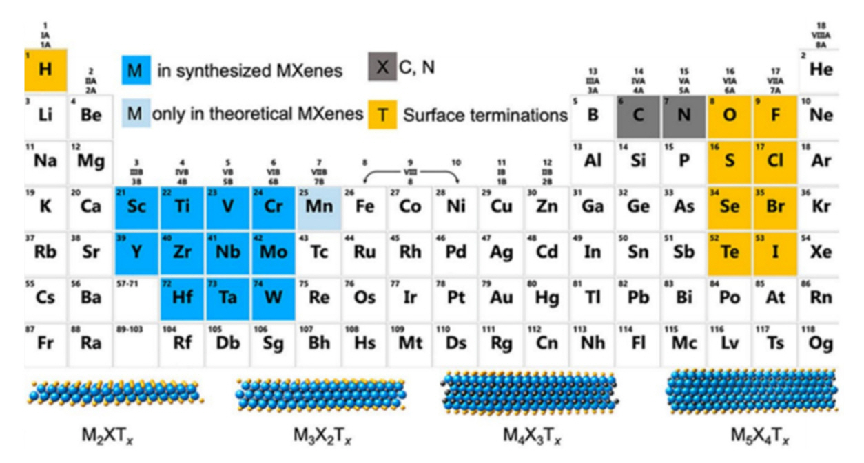


Research Trends in Electromagnetic Shielding using MXene-based Composite Materials


Fig. 1. A periodic table color-coded to indicate the composition of MXenes and a classic diagram of the MXene structure [14].
Fig. 2. possible MA mechanisms for the ZFO@PANI composite material [21].
Fig. 3. possible MA mechanisms for the ZFO@PANI composite material [27].
Fig. 4. σ (a–c) and EMI SET (a'–c') values of the rGMH/epoxy nanocomposite materials with different cell sizes; σ (d) of the rGMH-5 (MXene 90g/L including) nanocomposite materials at different directions; σ (e) and EMI SET (e') values of the rGM/epoxy nanocomposite materials [43].
Fig. 5. (a) SET, (b) SEA, (c) SER of rGO/MXene-x. (d) and (e) The average EMI SE of rGO/MXene-x. (f) The SSET of rGO/MXene-x. (g) Electromagnetic shielding mechanism diagram of rGO/MXene-x [44].
Fig. 6. Three-dimensional RL–f curves of (a) NiMG, (b) NiMR-A, and (c) NiMR-H aerogels. Comparison of EMA performances for (d) a NiMR-H aerogel in the parallel direction, vertical direction, and disordered state and (e) NiMR-H aerogels with different MXene to GO ratios (NiM-H, NiM3R1-H, NiM2R1-H, NiM1R2-H, NiM1R3-H, and NiR-H correspond to ratios of 1:0, 3:1, 2:1, 1:2, 1:3, and 0:1, respectively). (f) Statistics of RLmin and EABmax for different NiMR-H aerogels [45].
Fig. 7. Schematic illustration of EMW absorption mechanism for NiCo/TiC/TiO/CNTs [46].
Fig. 8. (a) Plots of electrical conductivity vs MXene content for MCAs. (b) Resistance change rates of MCA-1 during compression cycles at different strains. (c) Plots of EMI shielding effectiveness of MCAs. (d) EMI shielding performances of MCA-1 with different densities at the thickness of 2 mm. (e) Comparison of EMI shielding performances of MCA (red stars) and those of EMI shielding nanomaterials reported in the literature. (f) Schematic of EMI shielding mechanisms of MCA [48].
Fig. 9. (a) Electrical conductivities of the M@W nanocomposite aerogel, (b) EMI shielding efficiencies of the M@W nanocomposite aerogel, (c) average EMI shielding effectiveness of the M@W nanocomposite aerogel, (d) EMI SE/r of the M@W nanocomposite aerogel c, (e) the comparison of M@W nanocomposite aerogel with other reported materials, and (f) the proposed illustration of the shielding mechanism for the M@W nanocomposite aerogel at parallel growth direction [52].
Fig. 10. (a) r, (b) EMI SET, (c) SE/q and (d) SEA & SER of natural wood, WPC-500, WPC-1000 and WPC-1500 (WPC-carbonization degree) [54].
Fig. 11. Frequency dependence of (a) ε', (b) ε'', (c) μ', (d) μ'', (e) Tanδε, and (f) Tanδμ of Ti3C2Tx, Co9S8/C, Co9S8/C/Ti3C2Tx-50, Co9S8/C/Ti3C2Tx-100 and Co9S8/C/Ti3C2Tx-150 [55].
Fig. 12. Schematic illustration of the possible electromagnetic absorption mechanism of Co9S8/C/Ti3C2Tx-100 [55].
Fig. 13. Electromagnetic parameters of pure MXene film, MFC-1 (MXene and nanoplate like FeCo) and MFC-2 (MXene and nanoflower like FeCo) samples: (a) real and (b) imaginary part of complex permittivity, (c) dielectric loss tangent, (d) real and (e) imaginary part of complex permeability, and (f) magnetic loss tangent [60].
Fig. 14. (a, e) TEM images, (b, f) off-axis electron holograms, (c, g) magnetic flux lines and (d, h) schematic illustration of nanoflower-like FeCo alloy; (i) schematic illustration of MFC-2 [60].
Fig. 15. The main preparation process of NiCo-LDH/MXene hybrids [62].
Fig. 16. real part (a) and imaginary part (b) of complex permittivity of the six samples; real part (c) and imaginary part (d) of complex permeability of the six samples; dielectric loss tangent (e) and magnetic loss tangent (f) of the six samples [62].
Fig. 17. Illustration of EMW absorbing mechanism in the NiCo-LDH/MXene [62].
Fig. 18. (a) Shielding performance of MXene/Ni hybrids with different Ti3C2Tx contents ranging from 10 to 50wt % and (b) the corresponding average value of SEtotal, SEA, and SER of 2–18GHz, (c) the SEtotal curve of Ni-50% MXene with different thicknesses, and (d) the corresponding average value of SEtotal, SEA, and SER [34].
Fig. 19. The schematic diagram of preparation process of FMCM [70].
Fig. 20. 3D RL and contour map of the samples with different thicknesses (1.0–5.0mm) from 2.0 to 18.0GHz: Ti3CNTx (a, b), Ti3CNTx/HCF hybrids (d, e) and HCF (g, h); RLmin for Ti3CNTx, Ti3CNTx/HCF hybrids and HCF (c); the quarter wavelength thickness matching of Ti3CNTx/HCF hybrids (f, i) [71].
Fig. 21. (a) Sheet resistances and (b) EMI shielding performances of (MAX)n silk textile with different spray cycles and concentrations. (c) Plots of EMI SE versus spray cycles for (MA0.8)n silk textile. (d) Synergistic effect of AgNW and MXene on the EMI SE and the sheet resistances of functional silk textiles. (e) EMI shielding performances of (MA1)10 silk textile with different thicknesses. (f) EMI shielding performances and sheet resistances of (MA1)10 textiles with different textile substrate (silk, cotton, nylon, and wool) [72].
Fig. 22. (a) Schematic illustration of the preparation process of the d-MA film. Inset is a close-up photo of the d-MA film. (b) EMI shielding performances of AgNW, MA2m/2n, and d0.2-MAm/n films at various AgNW densities. Both MA2m/2n and dx-MAm/n films possess the same loading density. (c) Transmittances of MA films with different AgNW densities. (d) Relative transmittances of MA20/164 and d-MA10/82 films with various gap distances. (e) EMI shielding performances of MA films with various gap distances. (f) Experimental and simulated SE values for MA and d-MA films with various gap distances. (g) Schematic of the EMI shielding mechanisms of a d-MA film [74].
Fig. 1.
Fig. 2.
Fig. 3.
Fig. 4.
Fig. 5.
Fig. 6.
Fig. 7.
Fig. 8.
Fig. 9.
Fig. 10.
Fig. 11.
Fig. 12.
Fig. 13.
Fig. 14.
Fig. 15.
Fig. 16.
Fig. 17.
Fig. 18.
Fig. 19.
Fig. 20.
Fig. 21.
Fig. 22.
Research Trends in Electromagnetic Shielding using MXene-based Composite Materials
TOP
