
Articles
- Page Path
- HOME > J Korean Powder Metall Inst > Volume 22(3); 2015 > Article
-
ARTICLE
양극산화 알루미나 주형 기반의 전해 증착법을 이용한 니켈 나노선의 합성 및 특성 연구 - 임효령, 좌용호, 이영인a,*
- Synthesis and Characterization of Nickel Nanowires by an Anodic Aluminum Oxide Template-Based Electrodeposition
- Hyo-Ryoung Lim, Yong-Ho Choa, Young-In Leea,*
-
Journal of Korean Powder Metallurgy Institute 2015;22(3):216-220.
DOI: https://doi.org/10.4150/KPMI.2015.22.3.216
Published online: May 31, 2015
한양대학교 융합화학공학과
서울과학기술대학교 신소재공학과
Department of Fusion Chemical Engineering, Hanyang University, Ansan 426-791, Korea
a Department of Materials Science and Engineering, Seoul National University of Science and Technology, Seoul 139-743, Korea
- *Corresponding author : Young-In Lee, TEL: +82-2-970-6646, FAX: +82-2-973-6657, youngin@seoultech.ac.kr
© The Korean Powder Metallurgy Institute All rights reserved
This is an Open-Access article distributed under the terms of the Creative Commons Attribution Non-Commercial License (http://creativecommons.org/licenses/by-nc/3.0) which permits unrestricted non-commercial use, distribution, and reproduction in any medium, provided the original work is properly cited.
- 1,106 Views
- 2 Download
Abstract
- Vertically oriented nickel nanowire arrays with a different diameter and length are synthesized in porous anodic aluminium oxide templates by an electrodeposition method. The pore diameters of the templates are adjusted by controlling the anodization conditions and then they are utilized as templates to grow nickel nanowire arrays. The nickel nanowires have the average diameters of approximately 25 and 260 nm and the crystal structure, morphology and microstructure of the nanowires are systematically investigated using XRD, FE-SEM and TEM analysis. The nickel nanowire arrays show a magnetic anisotropy with the easy axis parallel to the nanowires and the coercivity and remanence enhance with decreasing a wire diameter and increasing a wire length.
- 나노재료(nanomaterial)는 벌크 재료와 비교하여 독특한 물리적, 화학적 성질들을 가지고 있기 때문에, 최근 나노 재료의 제조 및 응용에 관한 연구가 활발히 진행되고 있 다. 특히 그 중에서도 1차원 나노재료는 크기효과 뿐만 아 니라, 1차원 구조에 의해 발현되는 새로운 성질과 큰 비표 면적 및 소자로의 제작이 용이하다는 장점으로 인해 활발 하게 연구가 진행되고 있다[1-4]. 다양한 1차원 나노재료 중 강자성(ferromagnetic)을 갖는 금속 나노선(nanowire)은 큰 종횡비(aspect ratio)에 의해 길이 방향으로 자화용이 축 (magnetization easy axis)이 형성되고, 이를 통해 형상자기 이방성(shape anisotropy)을 나타내어 고밀도 수직자화 기 록매체(high density perpendicular magnetic recording media) 에 적합한 자기적 성질을 기대할 수 있다.
- 이와 같은 기록매체의 고밀도화, 소형화를 위해서는 강 자성 나노선을 제한된 면적에 고밀도로 정렬된 형태로 제 조할 수 있는 공정이 요구된다. 산성 전해질에서 알루미늄 (Al)을 양극산화(anodization) 처리하여 제작되는 양극산화 알루미늄(Anodic aluminum oxide, AAO) 주형(template)은 수직으로 배향된 규칙적인 고밀도(1011~1013/cm2)의 나노 기공을 가지고 있고 기공의 크기 및 간격을 제어하기가 용이하기 때문에 다양한 금속 및 산화물 나노선을 제조하 는 데 응용되고 있다[5-7]. 특히 간단하고 대량생산이 용 이한 전해증착(electrochemical deposition) 공정을 통해 주 형 내부에 나노선을 성장시키는 방법을 이용하면, 고밀도 로 정렬된 금속 나노선을 직경 및 길이를 정밀하게 제어 하여 합성할 수 있기 때문에 많은 주목을 받고 있다. 최근 상기의 공정을 이용하여 니켈(nickel), 철(iron), 코발트 (cobalt)와 같은 강자성 나노선의 제조에 대한 연구가 진행 되고 있다[8-10]. 하지만 나노선의 직경 제어 및 전해증착 전압, 온도 및 시간에 따른 나노선의 성장 거동에 대한 연 구가 주로 이루어지고 있으며[10, 11], 나노선의 직경, 길 이와 자기이방성 및 각형비(Squareness rato)의 상관관계에 대한 연구는 미비한 실정이다.
- 본 연구에서는 양극산화알루미나(Anodic Aluminum Oxide, AAO) 주형을 제조하고, 주형 내에 니켈(nickel)을 전해증착 공정(electrochemical deposition)을 이용하여 성 장시킴으로써 직경 및 길이가 제어된 니켈 나노선을 합성 하였다. 이와 같이 합성된 니켈 나노선의 결정구조, 형상 및 직경, 미세 구조와 자기적 특성을 체계적으로 관찰하였 고, 이를 통해 니켈 나노선의 결정학적, 형상학적 특성과 자기적 특성에 대한 상관관계를 고찰하였다.
서 론
- 나노선을 합성하기 위한 AAO 주형은 알루미늄박(두께: 0.13 mm, 99.99%, Aldrich)을 양극산화(anodizing)하여 제 조하였다. 시편 표면의 유기물 및 불순물을 제거하기 위해 아세톤 용액에 침지하여 10 분간 초음파로 세척한 후, 과 염소산과 에틸알콜을 혼합한 용액에서 150 mA/cm2의 전 류를 인가하여 3분간 전해연마를 실시하여 산화층을 제거 하였다. 약 30 nm의 평균 기공크기를 갖는 AAO를 제조 하기 위해, 1.8M의 황산을 전해질로 사용하여 표 1의 조 건으로 양극산화를 실시하였다. 1차 양극산화 후에 생성 되는 불규칙한 배열을 갖는 기공은 1.8 wt.% 크롬산과 6 wt.%의 인산이 용해된 용액에 1 시간동안 침지하여 제거 하였고, 2차 양극산화 이후에는 0.1 M 염화구리와 20 vol% 염산용액을 이용하여 잔류 알루미늄을 제거하였다. 최종적으로 주형 하부에 존재하는 barrier 층을 제거하기 위한 pore widening을 5 wt%의 인산용액에 20분 간 침지 하여 실시하였다. 200 nm의 평균 기공크기를 갖는 AAO 는 상용 제품(Anodisc 13, Wattmann)을 사용하였다. 제작 한 주형의 형상 및 기공 크기는 전계 방출 주사 현미경 (field emission scanning electron microscopy, FE-SEM, Hitachi S-4800)을 이용하여 분석하였다.
- Anodization conditions for the fabrication of anodic aluminum oxide templates with different pore size.
- AAO 내에 니켈을 전해증착하기 위해 주형 한쪽 면에 약 200 nm 두께의 금(Au)을 스퍼터링(sputtering)하여 전 기도금 시드(seed) 층을 형성하였다. 작업 전극(working electrode)은 주형을 알루미늄박에 고정시킨 후, 테프론 지 그(zig)를 이용하여 주형을 제외한 다른 부분이 전해질과 접촉되지 않도록 하여 제작하였으며, 상대전극(counter electrode)은 티타튬(Ti)에 백금(Pt)이 코팅된 바(bar)를 사 용하였다. 니켈의 전해도금을 위한 전해질은 pH가 4로 적 정된 1M NiSO4 + 0.4M H3BO3 + 0.2M NiCl2의 혼합용액 을 사용하였다. 전해도금은 작업전극과 상대전극을 연결 하고, 일정 전위기(potentiostat)를 이용하여 10 mA/cm2의 정전류(constant current)를 인가하여 상온에서 2시간 동안 진행하였다. 전해 증착된 나노선의 결정구조, 형상 및 직 경, 미세구조는 X-선 회절분석기(X-ray diffractometer, XRD, Rigaku D/MAX-2500)와 FE-SEM, 투과전자현미경 (transmission electron microscopy, TEM, JEOL JEM-2100F) 을 이용하여 관찰하였다. 나노선의 자성 특성은 상온에서 진동시료자력계(vibrating sample magnetometer, VSM, LakeShore VSM 7410)를 이용하여 측정하였다.
실험방법
| Electrolyte | Anodizing | Voltage | Time | Temp. |
|---|---|---|---|---|
|
|
||||
| 1.8 M H2SO4 | 1st | 15 V | 30 min | 1°C |
| 2nd | 20 V | 3 h 30 min | 1°C | |
- 그림 1은 상용 AAO 주형과 황산을 전해질로 사용하여 제작한 주형의 기공을 보여주는 FE-SEM 분석 결과이다. 매우 균일한 크기의 기공이 형성된 것을 알 수 있으며, 상 용 주형은 약 260 nm의 평균 기공크기(기공도: 52%)를 나 타내었고, 황산에서 제작된 주형의 평균 기공 크기는 약 25 nm(기공도: 27%)로 확인되었다. 상기와 같이 준비된 AAO 주형 내에 전해도금을 이용하여 니켈을 증착하고, 제조된 나노선의 결정구조 분석 결과를 그림 2에 나타내 었다. AAO 주형은 비정질 구조이기 때문에 회절 패턴을 관찰할 수 없었으며, 주형 내에 성장된 나노선은 기공크기 와 관계없이 모두 면심입방구조(face-centered cubic)의 니 켈(JCPDS no. 70-1849)로 확인되었다. 니켈 나노선을 구 성하는 결정면의 배향(preferred orientation)은 결정자기이 방성에 영향을 미치기 때문에 아래 식 (1)에 의해 배향계 수(texture coefficient)를 계산하여 확인하였고, 그 결과를 표 2에 정리하였다.
- Anodization conditions for the fabrication of anodic aluminum oxide templates with different pore size.
- 상기 식에서 Im(hkl)과 I0(hkl)은 각각 면에 해당하는 회 절피크의 측정 강도와 표준 강도(JCPDS no. 70-1849)를 나타내며, n은 총 회절피크의 수를 의미한다. Tc의 범위는 0 에서부터 n이며, n은 특정한 결정면으로의 완전한 배향 을 의미하고 1은 완전 불규칙 배향을 나타낸다. 표 2에서 와 같이, 전해 증착된 니켈 나노선은 (111) 면으로 우선 성 장한 것을 알 수 있으며, 25 nm의 평균 기공 크기를 갖는 AAO를 통해 합성된 나노선은 260 nm의 경우에 비해 더 욱 큰 배향계수를 갖는 것으로 확인되었다.
- 그림 3는 전해 증착된 니켈 나노선의 형상, 직경 및 길 이를 보여주는 FE-SEM 분석 결과이다. 합성된 나노선은 기공을 따라 성장되어 종횡비가 큰 1차원 형상을 가지고 있었으며, 대체적으로 균일한 직경과 길이를 나타내었다. 나노선의 직경은 주형의 기공과 동일한 크기를 나타내었 고, 평균 길이는 각각 27 μm (직경: 260 nm)와 24 μm (직경: 25 nm)로 확인되었다. 나노선의 길이는 전해 증착 시간을 조절하여 제어되었고, 이를 그림 3(E)에 나타내었 다. 증착 시간이 증가할수록 나노선의 길이는 증가하였으 며, 평균 기공 크기 260 nm와 25 nm 주형을 이용하였을 경우, 각각 시간 당 13.2 μm와 11.8 μm의 성장속도를 나 타내었다.
- 그림 4는 전해 증착된 구리 나노선의 미세구조를 관찰 하기 위해 AAO 주형을 5M NaOH 용액으로 제거한 후에 실시한 TEM 분석 결과이다. 각각의 나노선은 그림 3에서 와 유사한 평균 직경과 치밀한 미세구조를 갖는 것으로 확인되었다. 그림 4(B)의 보여주듯이, 260 nm의 직경을 갖는 나노선은 제한 시야 회절 패턴(selected area diffraction pattern, SAED) 분석에 의해 링(ring)패턴이 나타나 다결정 성을 갖는 것으로 확인되었으며, 반면에 25 nm의 평균직 경을 갖는 나노선은 점(dot) 형식의 SAED 패턴이 관찰되 어 전해 증착된 니켈 나노선은 단결정으로 성장되었음을 알 수 있었고, 우선 성장방향은 그림 4(D)의 고분해능 (high resolution) 사진 및 고속푸리에변환(fast Fourier transform) 결과로부터[111] 방향으로 확인되었다. 이는 앞 선 XRD 분석에서의 배향계수와 잘 일치하는 결과이며, 전해질 내의 Ni2+ 이온이 작업전극에서 환원될 때, 미세한 기공 크기로 인해 상대적으로 제한된 핵생성(nucleation) 숫자와 속도에 따른 결정성 차이로 사료된다[12].
- 그림 5(A)와 (B)는 직경이 각각 260 nm와 25 nm인 니 켈 나노선의 자기이력곡선(hysteresis loop)을 나타낸 그래 프이며, 자기장을 나노선의 길이 방향에 수평(H⊥)과 수직 (H∣∣)방향으로 각각 인가하여 분석한 결과이다. 표 3에는 자기이력곡선으로부터 얻은 각형비(squareness ratio)와 보 자력을 정리하여 나타내었다. 직경이 260 nm인 나노선의 경우, 수평과 수직방향의 자기장에 대해 유사한 자기이력곡 선과 각형비(squareness ratio)를 나타내었고, 이를 통해 나노 선의 길이방향으로 자화용이 축(easy axis of magnetization) 이 존재하지 않는 것을 확인하였다. 반면에 그림 5(B)에서 와 같이 직경이 25 nm인 나노선의 경우에는 나노선의 길 이방향으로 수평하게 자기장을 인가한 경우가 수직한 방 향에 비해 명확하게 증가한 보자력과 각형비를 갖는 것으로 확인되어 나노선과 수평한 방향으로 자화용이 축이 존재하 는 것을 알 수 있다. 그림 5(C)는 나노선의 길이가 자기적 성 질에 미치는 영향을 확인하기 위해 25 nm의 기공크기를 갖 는 주형에 30분간 니켈을 전해 증착하여 약 6 μm의 길이를 갖도록 제조된 나노선의 자기이력곡선이다. 상대적으로 작은 종횡비를 가짐에도 불구하고, 260 nm의 나노선과의 비교를 통해 자화용이 축이 형성된 것으로 확인되었지만, 동일한 직경의 24 μm의 길이를 갖는 나노선에 비해서는 작은 각형비 및 보자력을 나타내었다. 이러한 결과는 합성 된 니켈 나노선의 직경, 길이 및 미세구조에 의한 결정 자 기이방성과 형상 자기이방성의 차이로 해석할 수 있다. 즉, 다자구(multi-domain), 다결정성이 존재하는 큰 직경의 니 켈 나노선은 자기이방성을 발현하지 못하지만, 단일 자구 (single domain)의 크기와 유사한 직경 및 단결정성을 갖 는 니켈 나노선의 수평방향으로는 자화용이 축이 형성되 어 큰 각형비와 보자력을 나타내고, 이러한 특성은 나노선 의 길이가 길어짐에 따라 형상자기이방성이 강하게 작용 하여 각형비와 보자력이 더욱 개선되는 것으로 해석할 수 있다.
결과 및 고찰
| Ni nanowires into AAO (25 nm) | Ni nanowires into AAO (260 nm) | ||
|---|---|---|---|
|
|
|||
| hkl | Tc | hkl | Tc |
|
|
|||
| (111) | 2.01 | (111) | 1.33 |
| (200) | 0.49 | (200) | 0.96 |
| (220) | 0.51 | (220) | 0.71 |
Top views of anodized alumina templates fabricated by two step anodization. (A, B) commercial AAO template fabricated by Whatman Inc., average pore diameter of 260 nm, (C, D) 1.8M sulfuric acid, average pore diameter of 25 nm. (B and D) are high magnification image of (A and C), respectively.

XRD patterns of the electrodeposited nanowires into the AAO templates with average diameters of (A) 260 nm and (B) 25 nm.

FE-SEM images of the electrodeposited nickel nanowires into the AAO templates with average diameters of (A and B) 260 nm and (C and D) 25 nm, (E) is the graph showing a nanowire growth length as a function of electrodeposition times.

TEM images and SAED patterns of the electrodeposited nickel nanowires into the AAO templates with average diameters of (A and B) 260 nm and (C and D) 25 nm.


- 고밀도 수직자화 기록매체를 실현하기 위해서는 강자성 나노선을 제한된 면적에 고밀도로 정렬된 형태로 제조할 수 있는 공정이 필요하다. 이를 위해 본 연구에서는 균일 한 크기의 미세 기공을 갖는 AAO 주형 내에 전해증착 공 정을 통해 니켈 나노선을 성장시키고, 나노선의 결정성, 직경 및 길이에 따른 자기이방성을 고찰하였다. 미세한 직 경, 큰 종횡비와 단결정성을 갖는 경우가 그렇지 않는 경 우와 비교하여 우수한 보자력과 각형비를 나타내어 큰 자 기 이방성을 갖는 것으로 확인되었고, 특히 25 nm의 직경 과 24 μm의 길이를 갖고 [111] 방향으로 우선 성장된 단 결정 니켈 나노선은 길이방향으로 751 Oe의 보자력과 0.45의 각형비를 나타내어, 추후 합금화와 미세구조 최적 화를 통해 수직자화기록매체로의 응용이 가능하다고 사료 된다.
결 론
-
Acknowledgements
- 이 연구는 서울과학기술대학교 교내연구비의 지원으로 수행되었습니다.
감사의 글
- 1. Y Xia and P Yang, Adv. Mater. (2003) 15 351.Article
- 2. M Law, J Goldberger and P Yang, Annu. Rev. Mater. Res. (2004) 34 83.Article
- 3. G Shen, PC Chen, K Ryu and C Zhou, J. Mater. Chem. (2009) 19 828.Article
- 4. HY Yue, S Huang, EJ GuO, LP Wang, FW Kang, ZM Yu, YK Guo and FL Sun, J. Korean Powder Metall. Inst. (2011) 18 14.Article
- 5. H Masuda and K Fukuda, Science. (1995) 268 1466.Article
- 6. L Yi, L Zhiyuan, C Shuoshuo, H Xing and H Xinhua, Chem. Commun. (2010) 46 309.Article
- 7. SJ Sim, KK Cho and YY Kim, J. Korean Powder Metall. Inst. (2011) 18 49.Article
- 8. V Vega, T Böhnert, S Martens, M Waleczek, JM Montero-Moreno, D Görlitz, VM Prida and K Nielsch, Nanotechnology. (2012) 23 465709.Article
- 9. R Lavín, JC Denardin, J Escrig, D Altbir, A Cortés and H Gómez, J. Appl. Phys. (2009) 106 103903.
- 10. C Li, C Ni, W Zhou, X Duan and X Jin, Mater. Lett. (2013) 106 90.Article
- 11. T Gao, GW Meng, J Zhang, YW Wang, CH Liang, JC Fan and LD Zhang, Appl. Phys. A. (2001) 73 251.ArticlePDF
REFERENCES
Figure & Data
References
Citations
 Cite this Article


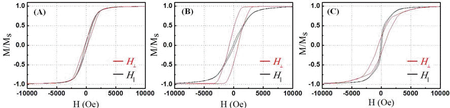


Fig. 1.
Fig. 2.
Fig. 3.
Fig. 4.
Fig. 5.
| Electrolyte | Anodizing | Voltage | Time | Temp. |
|---|---|---|---|---|
|
|
||||
| 1.8 M H2SO4 | 1st | 15 V | 30 min | 1°C |
| 2nd | 20 V | 3 h 30 min | 1°C | |
| Ni nanowires into AAO (25 nm) | Ni nanowires into AAO (260 nm) | ||
|---|---|---|---|
|
|
|||
| hkl | Tc | hkl | Tc |
|
|
|||
| (111) | 2.01 | (111) | 1.33 |
| (200) | 0.49 | (200) | 0.96 |
| (220) | 0.51 | (220) | 0.71 |
| Sample | Diameter | Length | Field | Squareness ratio | Coercivity |
|---|---|---|---|---|---|
|
|
|||||
| Fig. |
260 nm | 27 μm | H⊥ | 0.11 | 240 Oe |
| H|| | 0.08 | 131 Oe | |||
| Fig. |
25 nm | 24 μm | H⊥ | 0.45 | 751 Oe |
| H|| | 0.05 | 141 Oe | |||
| Fig. |
25 nm | 6 μm | H⊥ | 0.22 | 497 Oe |
| H| | 0.15 | 90 Oe | |||
Table 1.
Table 2.
Table 3.
TOP
