 KPMI
KPMI

Articles
- Page Path
- HOME > J Powder Mater > Volume 33(4); 2026 > Article
-
Research Article
- Fabrication of Multilayer Core-Shell Structure for High Power Factor in Bi2Te2.7Se0.3 Thermoelectrics
-
Su Min Eun1, Jin Kyeong Shin1, Se Been Jeong1, Eui Seon Lee1, Sung-Tag Oh1,2, Byung Joon Choi1,2,*

-
Journal of Powder Materials 2026;33(4):299-309.
DOI: https://doi.org/10.4150/jpm.2026.00192
Published online: August 31, 2026
1Department of Materials Science and Engineering, Seoul National University of Science and Technology, Seoul 01811, Republic of Korea
2The Institute of Powder Technology, Seoul National University of Science and Technology, Seoul 01811, Republic of Korea
- *Corresponding author: Byung Joon Choi E-mail: bjchoi@seoultech.ac.kr
© The Korean Powder Metallurgy & Materials Institute
This is an Open Access article distributed under the terms of the Creative Commons Attribution Non-Commercial License (http://creativecommons.org/licenses/by-nc/4.0/) which permits unrestricted non-commercial use, distribution, and reproduction in any medium, provided the original work is properly cited.
- 437 Views
- 7 Download

Abstract
- Bi₂Te₃-based thermoelectric materials are attractive near room temperature, but their performance is constrained by sensitive carrier-concentration control, strong crystallographic anisotropy, and compositional instability from volatile Te. Here, a multilayer core-shell structure was fabricated by conformally coating Bi₂Te₂.₇Se₀.₃ (BTS) powders with ZnO–TiO₂ layers using rotary-type powder atomic layer deposition (pALD), followed by spark plasma sintering. Two configurations with the same ~4 nm total oxide thickness were prepared: a ZnO/TiO₂ bilayer (ZT) and a ZnO/TiO₂/ZnO/TiO₂ multilayer (DZT), where multilayer denotes the deposition scheme rather than a directly imaged layered architecture. Electron microscopy confirmed uniform amorphous shells that were retained as continuous interfacial films after sintering. The oxide interfaces donated electrons to the matrix, raising the carrier concentration and effective mass while preserving mobility and thereby enhancing the electrical conductivity and power factor; simultaneously they scattered phonons and suppressed bipolar conduction, lowering the lattice thermal conductivity. DZT achieved the highest power factor, attributed to its different deposition configuration, whereas ZT exhibited the lowest thermal conductivity; the two coated specimens reached comparable figures of merit (zT) within the measurement uncertainty, both markedly exceeding uncoated BTS. ALD-based interface engineering thus decouples electronic and phononic transport in n-type Bi₂Te₃.
- Bi-Te-based thermoelectric materials possess a layered structure held together by van der Waals bonding and exhibit strong anisotropy, delivering excellent thermoelectric performance near room temperature [1-6]. Owing to these characteristics, they have attracted considerable attention as materials suited to low-temperature applications such as wearable devices, self-powered IoT technologies, sensors, and medical devices [7-9]. Through diverse approaches such as nanostructuring, band and defect engineering, and texturing, high performance with zT exceeding ~1.5 has been reported for p-type Bi2Te3 [10]. However, for n-type Bi2Te3, performance enhancement remains limited compared with the p-type counterpart owing to intrinsic material and processing constraints. Because n-type Bi2Te3 is based on a Te-rich composition with Se doping, it is vulnerable to compositional instability under high-temperature or long-term operation due to the high volatility of Te [4, 11, 12]. In addition, Bi2Te3 intrinsically exhibits p-type behavior because of Bi-Te antisite defects, so realizing n-type conduction requires precise control of a complex defect structure-including Te vacancies and antisite defects-together with extrinsic doping. As a result, the carrier concentration is highly sensitive to control, and the strong anisotropy along the c-axis must also be taken into account, making performance optimization even more challenging. Moreover, conventional bulk processes such as hot pressing and mechanical alloying expose the material to high temperatures for extended periods, making it difficult to stably maintain the microstructure and composition [13, 14]. Therefore, the development of a new process capable of precisely controlling the structure and composition even at low temperatures is required.
- Atomic layer deposition (ALD) is a technique that forms uniform, atomic-scale thin films at low temperature, making it well suitable to the interface engineering of thermoelectric materials [15-20]. ALD is based on cycles of precursor dosing-purge-reactant dosing-purge, and the reaction proceeds in a self-limiting manner through surface saturation, enabling precise control of the film thickness, composition, and uniformity. It also allows uniform coating even on irregular powder surfaces; the rotary-reactor-based powder ALD (pALD) process used in this study enables uniform dispersion regardless of powder size and density through agitation [21, 22]. However, because powder agglomeration during the process degrades the coating uniformity, controlling the process conditions to minimize it is important. When ALD-coated powders are sintered, new interfaces form within the sintered body, from which two main effects can be expected. At the interfaces between dissimilar materials with different band gaps, an energy-filtering effect arises in which low-energy carriers are selectively scattered by the barrier formed at the interface [23-25]. In n-type materials in particular, the interfacial barrier formed by the conduction-band offset filters carriers and increases the potential difference, thereby enhancing the Seebeck coefficient. However, if the barrier height is excessive the electrical conductivity decreases, whereas if it is too low the energy-filtering effect weakens; an appropriate band-structure design is therefore necessary. In addition, the newly formed interfaces induce phonon scattering, effectively reducing the lattice thermal conductivity. This increase in the Seebeck coefficient and decrease in the lattice thermal conductivity contribute to zT enhancement, and optimizing the carrier concentration can relieve the trade-off between the electrical and thermal conductivity.
- In this study, pALD-coated powders were consolidated by spark plasma sintering (SPS) to achieve rapid densification at a low process temperature, securing high mechanical stability and minimizing the loss of volatile elements. Furthermore, a ZnO–TiO2 multilayer coating with a high melting point and thermal stability was applied to compensate for the thermal instability of Bi2Te3, and the performance limitation caused by the decrease in electrical conductivity observed for single-layer TiO2 ALD was addressed through the multilayer structure.
1. Introduction
- 2.1 Fabrication of the core-shell structure and sintered body
- The raw powder was prepared by milling Bi2Te2.7Se0.3 (BTS) flakes in a three-dimensional mixer (3D mixer ball mill, DTB-2, DAEWHA TECH Global Co., Korea). The mass ratio of the 10-mm-diameter ZrO2 balls to the powder was 5:1, and dry milling was performed at room temperature for 5 h; the average particle size (D50) immediately after milling was approximately 1–4 µm. A ZnO-TiO2 multilayer was coated onto the powder surface by rotary-reactor-based thermal atomic layer deposition (Thermal ALD system, Atomic Shell, CN-1 Co., Korea) to fabricate the core-shell structure. To improve the dispersibility and coating uniformity, N2 gas was supplied at a flow rate of 200 sccm while the reactor was agitated at 30 rpm, and a 30-min preheating step was carried out. Diethylzinc (DEZ, Lake Material Co., Korea) and titanium isopropoxide (TTIP, I-CHEMS Co., Korea) were used as the precursors for ZnO and TiO2, respectively, with H2O as the reactant, and ~8 g of powder was loaded per process batch. The ZnO ALD process consisted of DEZ dosing (0.5 s)-N2 purge (15 s)-H2O dosing (0.5 s)-N2 purge (15 s), and the TiO2 ALD process consisted of TTIP dosing (1 s)-N2 purge (30 s)-H2O dosing (1.5 s)-N2 purge (30 s). The number of cycles for each process was set based on the growth per cycle (GPC) of ZnO and TiO2, which were 0.1 nm/cycle and 0.04 nm/cycle, respectively. The GPCs of the DEZ/H₂O and TTIP/H₂O processes were characterized in our previous work [19, 21-24, 26].
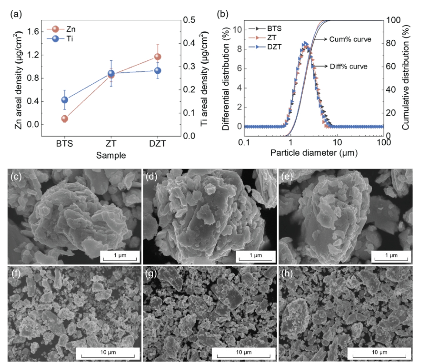
- For the single-bilayer (ZnO/TiO2) sample, 20 ZnO ALD cycles were first applied directly on the BTS surface to form a 2 nm ZnO layer, followed by 50 TiO2 ALD cycles to form a 2 nm TiO₂ outer layer, amounting to 70 cycles in total and a shell thickness of ~4 nm. For the double-bilayer (ZnO/TiO2/ZnO/TiO2) sample, the same oxide budget was subdivided into four layers deposited in the order ZnO (10 cycles, 1 nm) / TiO₂ (25 cycles, 1 nm) / ZnO (10 cycles, 1 nm) / TiO₂ (25 cycles, 1 nm, outermost), again giving 70 cycles and a total shell thickness of ~4 nm. Thus both samples prepared with an identical total number of ALD cycles and therefore with a nominally identical total oxide amount and total shell thickness; the two samples differ only in how the oxide is subdivided, i.e. in the number of internal ZnO–TiO₂ boundaries, and not in the quantity of oxide deposited. This is consistent with the comparable Zn and Ti areal densities measured by ED-XRF [Fig. 1(a)].
- The pALD-coated powder was consolidated into pellets by spark plasma sintering (SPS system, SPS-20, WELL TECH Co., Korea) using a graphite mold with a diameter of 15 mm and a height of 60 mm. Under a vacuum of 3.5 mTorr, the powder was heated to 673 K at a ramp rate of 80 K/min, held under a pressure of 50 MPa for 5 min, and then cooled under pressure. The fabricated pellets, approximately 4 mm in height, were mechanically polished with sandpaper from #200 to #2000 and machined using a diamond cutter. The prepared specimens were designated as the ZT sample with a BST/ZnO(2 nm)/ TiO2(2 nm) structure and the DZT (Double-ZT) sample with a BST/ZnO(1 nm)/TiO2(1 nm)/ZnO(1 nm)/TiO2(1 nm) structure, respectively.
- 2.2 Characterization
- The particle size distribution of the powders was measured using a laser diffraction particle size analyzer (LS 13 320, BECKMAN COULTER, USA). The microstructures of the powders and pellets were observed by high-resolution field-emission scanning electron microscopy (HR-FESEM, SU8010, Hitachi, Japan), focused ion beam (FIB, Carl Zeiss, Germany), and spherical-aberration-corrected scanning transmission electron microscopy (Cs-STEM, NEO ARM, JEOL, Japan), and the composition and chemical-bonding states were analyzed by energy-dispersive X-ray spectroscopy (EDS), energy-dispersive X-ray fluorescence (ED-XRF, ARL QUANTX, Thermo Fisher Scientific, USA), and X-ray photoelectron spectroscopy (XPS, Nexsa, Thermo Fisher Scientific, USA). Phase analysis was performed using X-ray diffraction (XRD, D8 Advance, Bruker, Germany) and fast Fourier transform (FFT) with Digital Micrograph (Gatan, Inc., USA). The electrical properties were measured using a Hall measurement system (HMS-3000, Ecopia, Korea) and a ZEM-3 system (M8, Ulvac, Japan), and the thermal conductivity and specific heat were measured by laser flash analysis (LFA, LFA447, NETZSCH, Germany). The thermoelectric figure of merit zT was calculated using
2. Experimental Section
- 3.1 Microstructure of the core-shell powders
- Fig. 1(a) shows the Zn and Ti areal densities upon pALD coating, measured by ED-XRF analysis. The ZT and DZT specimens exhibit a similar magnitude of increase relative to the background signal observed for the BTS specimen, indicating that a thin film of approximately 4 nm was uniformly deposited. In the particle size distribution of Fig. 1(b), all specimens exhibit a main peak near 2-2.2 µm, confirming that powder agglomeration and fracture caused by inter-particle collisions during the pALD process were effectively suppressed. In addition, the HRSEM analysis in Fig. 1(c-h) confirms that the pALD process did not induce any significant change in the morphology or size distribution of the individual particles. Such uniform particle morphology and size distribution are expected to contribute to a uniform dispersion of the interfaces during sintering. The EDS results in Table 1 confirm approximately 0.25 at% Zn and approximately 0.3 at% Ti in the ZT and DZT specimens, and the oxygen content also increased relative to BTS after pALD, supporting the successful deposition of the oxide thin films on the BTS powder surface. The Zn (0.21 vs. 0.29 at%) and Ti (0.27 vs. 0.31 at%) contents of ZT and DZT agree with each other to within the precision of the technique at these dilute levels and with the comparable Zn and Ti areal densities measured by ED-XRF [Fig. 1(a)], as expected for two specimens deposited with the same total number of ALD cycles. The oxygen contents (28.9, 43.1, and 32.8 at% for BTS, ZT, and DZT) do not follow this trend, because oxygen is the least reliable element to quantify in this configuration: the measured O signal also contains surface-adsorbed species, the native surface oxide of BTS, and adventitious contamination, and the electron interaction volume of SEM-EDS (~1 µm) is more than two orders of magnitude larger than the ~4 nm shell. The oxygen values are therefore taken as qualitative evidence of oxide formation, whereas the ED-XRF areal densities of Fig. 1(a) and the Cs-STEM shell thicknesses of Fig. 3 provide the quantitative basis for comparing the ZT and DZT specimens.
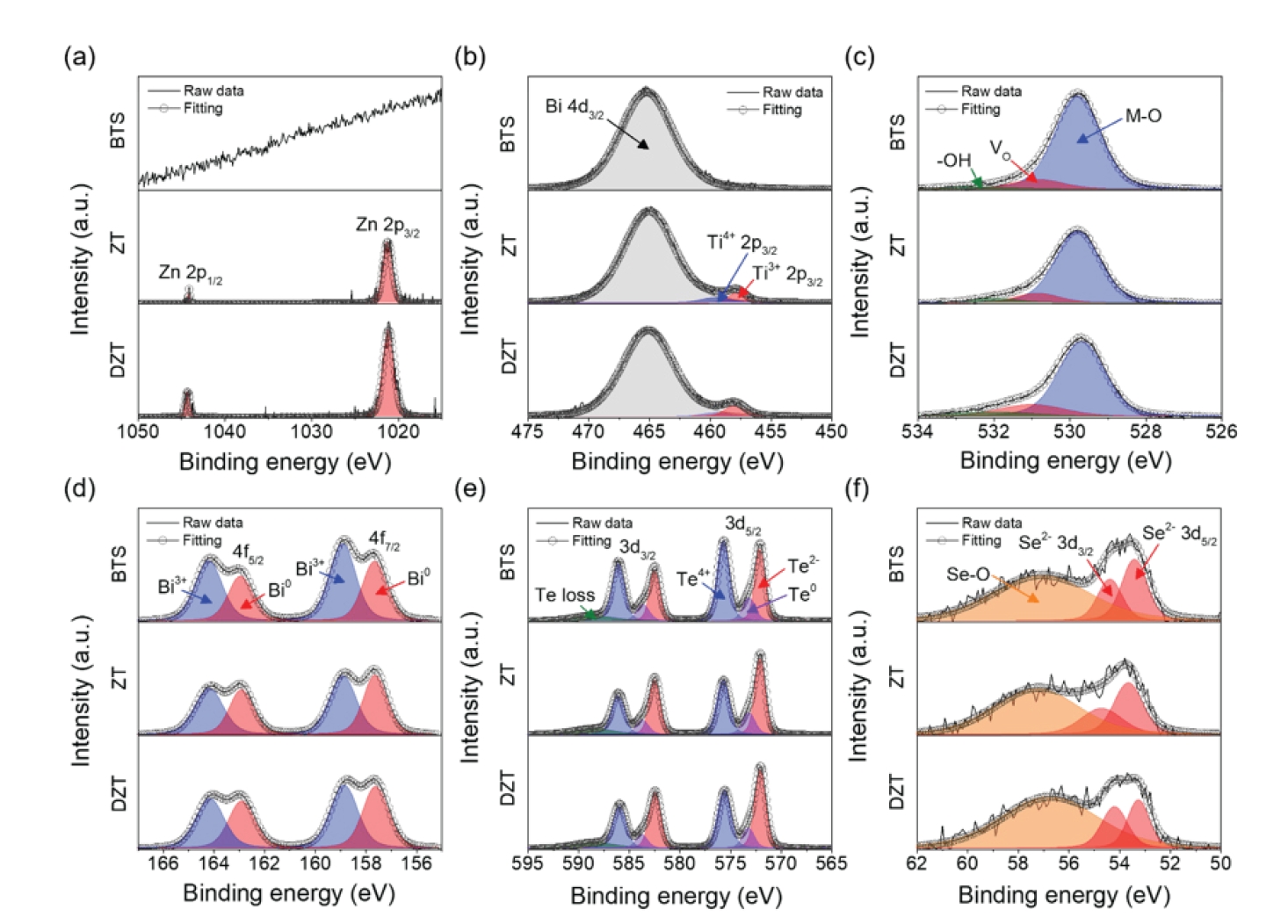
- Fig. 2 shows the XPS spectra for Zn 2p, Ti 2p, O 1s, Bi 4f, Te 3d, and Se 3d. The Zn 2p and Ti 2p spectra of the ZT and DZT specimens in Fig. 2(a,b) exhibit peaks corresponding to Zn-O and Ti-O bonding, respectively, confirming the formation of ZnO and TiO2 on the powder surface, and the O 1s spectrum of Fig. 2(c) shows an increased contribution from metal-oxygen bonding consistent with the oxide shell. For the matrix elements, the Bi 4f, Te 3d, and Se 3d spectra in Fig. 2(d-f) shift slightly toward lower binding energy in the coated specimens relative to BTS. This overall shift toward lower binding energy is interpreted as reflecting the charge compensation and n-type doping induced by electron transfer from the oxide layer to the BTS matrix during the pALD process [23, 24]. The trend is more pronounced for the DZT specimen, indicating a greater degree of interfacial charge transfer for the subdivided deposition configuration, consistent with the enhanced carrier concentration discussed below.
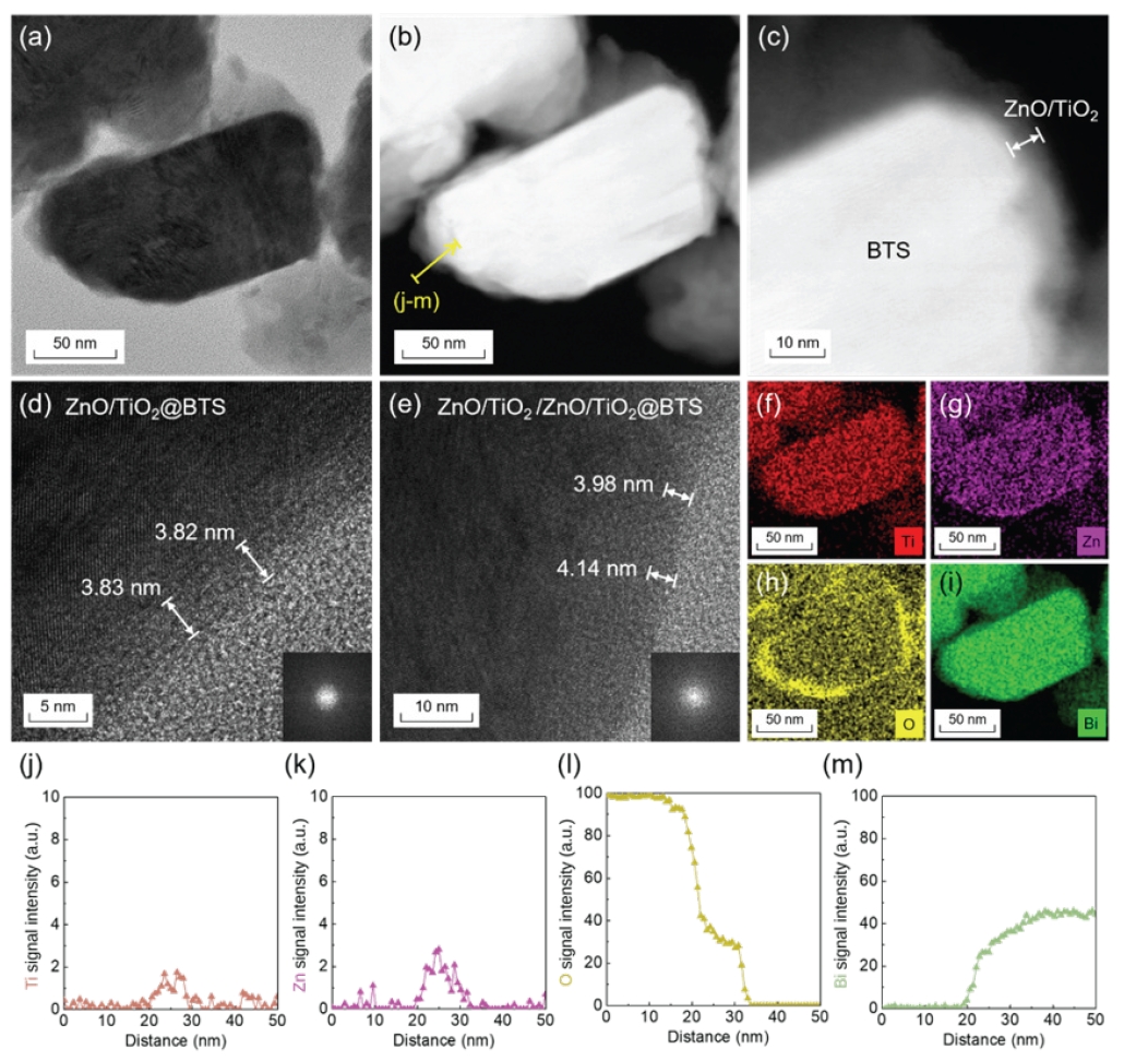
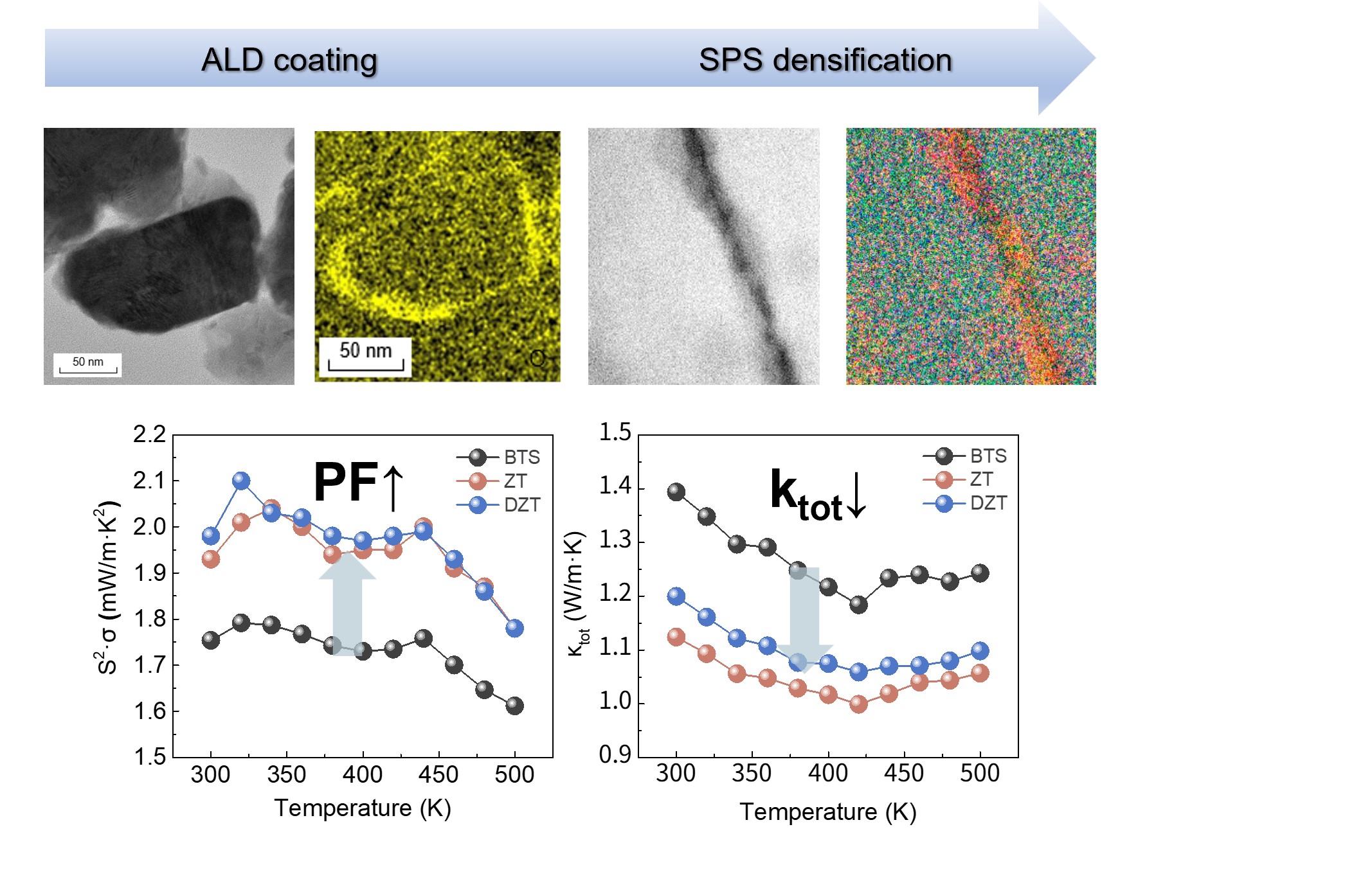
- The core-shell structure of the coated powders was examined in detail by Cs-STEM, as shown in Fig. 3. The TEM image of the ZT specimen [Fig. 3(a)] and the corresponding STEM images [Fig. 3(b,c)] reveal a continuous, conformal shell that uniformly covers the BTS core. While the high-magnification image [Fig. 3(c)] clearly confirms the core-shell architecture, the individual ZnO and TiO₂ sublayers are not distinctly resolved and instead appear as a single, uniform oxide shell on the BTS surface. The high-resolution TEM images of the surface regions [Fig. 3(d,e)] also show that the shell is amorphous, in contrast to the crystalline BTS core, as further confirmed by the diffuse rings in the FFT insets. The measured shell thicknesses were approximately 3.82-3.83 nm for the ZT specimen and 3.98-4.14 nm for the DZT specimen, in good agreement with the target thickness of ~4 nm and consistent with the ED-XRF results. The indistinguishability of the internal layer structure was observed in both the ZT and DZT specimens, indicating that although the core-shell geometry is well established, the intended multilayer stacking is not clearly discernible in the TEM/STEM images. This is an expected outcome rather than an unexplained absence: the atomic numbers of Zn (Z = 30) and Ti (Z = 22) are close, so the HAADF Z-contrast between the ZnO and TiO2 sublayers is intrinsically weak; both sublayers are amorphous, so that no lattice-fringe or diffraction contrast is available to distinguish them; and in the DZT specimen the individual sublayers are nominally only ~1 nm thick, comparable to the expected interdiffusion and intermixing length at the sublayer boundaries. A discretely resolved multilayer image should therefore not be expected even if the intended deposition sequence was faithfully executed. Accordingly, the term multilayer is used throughout this work to denote the deposition scheme, that is, the number of ZnO-TiO2 deposition steps, and not a layered architecture that has been directly imaged. The EDS elemental maps [Fig. 3(f-i)] show that Ti, Zn, and O are enriched at the particle surface while Bi is concentrated in the core, and the corresponding line profiles [Fig. 3(j-m)] confirm that the Ti, Zn, and O signals peak in the surface region and decrease toward the interior, whereas the Bi signal shows the opposite trend. These results demonstrate that a uniform, conformal ZnO-TiO2 shell was successfully formed on the BTS core by the pALD process.
- 3.2 Microstructure of the sintered green body
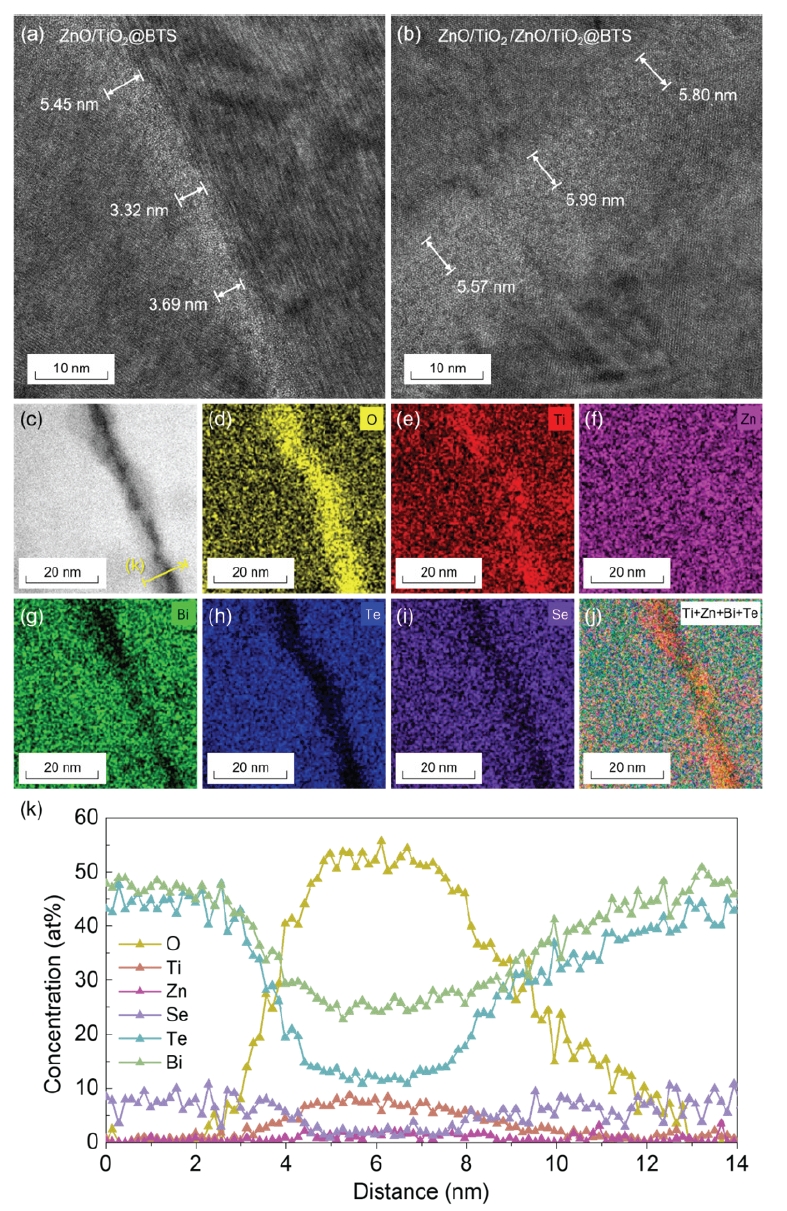
- To evaluate whether the core-shell interfaces are retained after consolidation, the sintered pellets were analyzed by Cs-STEM (Fig. 4). The TEM images of the interface regions [Fig. 4(a,b)] show that the amorphous oxide layers survive the SPS process and remain as continuous interfacial films between the BTS grains. In the ZT specimen in Fig. 4(a), the interfacial-layer thickness was approximately 3.3–5.5 nm, whereas the DZT specimen in Fig. 4(b) exhibited a thicker interfacial region of approximately 5.6–6.0 nm, consistent with its subdivided deposition configuration. The slightly larger thickness relative to the as-coated powders is attributed to the coalescence of shells from adjacent particles at the grain boundaries during sintering. The EDS elemental maps in Fig. 4(c-i) show that O and Ti are localized at the interface, forming a continuous oxide layer that delineates the BTS grains, while Bi, Te, and Se remain confined to the matrix; the overlay map in Fig. 5(j) clearly visualizes the oxide interface separating adjacent grains. The line profiles in Fig. 4(k) confirm the co-localization of O and Ti at the interface with a concomitant depletion of the matrix elements. These observations confirm that the ALD-derived oxide interfaces are thermally and structurally stable under SPS and are uniformly distributed throughout the sintered body, providing the interfacial network required for carrier filtering and phonon scattering.
- 3.3 Thermoelectric properties
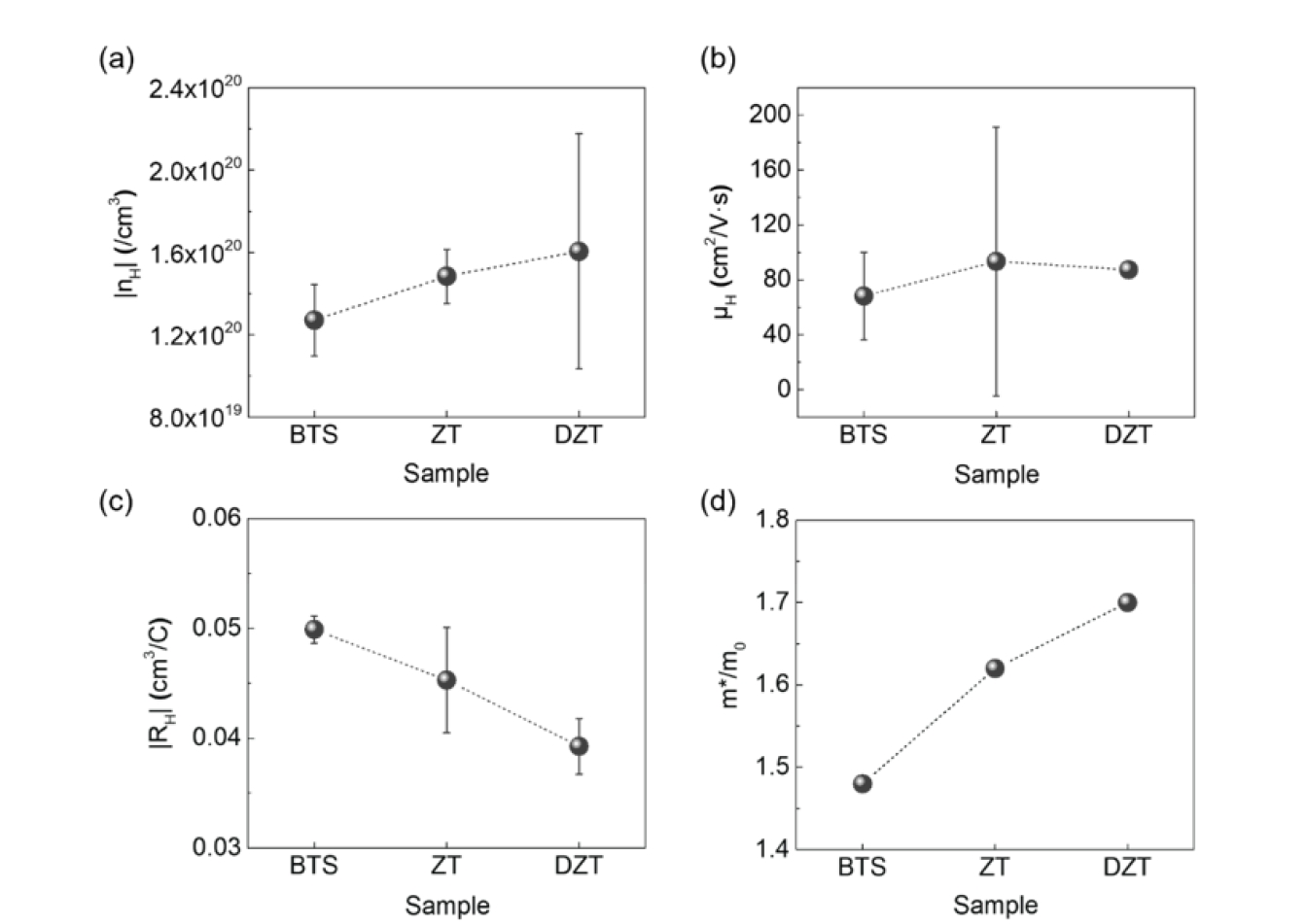
- The room-temperature Hall-effect measurement results are summarized in Fig. 5. The carrier concentration [Fig. 5(a)] showed a tendency to increase from approximately 1.3 × 1020 cm-3 for BTS to 1.5 × 1020 cm-3 for ZT and 1.6 × 1020 cm-3 for DZT, indicating that the oxide interfaces donate electrons to the BTS matrix and that this effect is stronger for the subdivided deposition configuration of DZT. Because the layered architecture could not be directly resolved (Fig. 3), the difference between ZT and DZT is attributed to the different shell composition, Zn-Ti intermixing, and interfacial chemistry produced by the subdivided deposition sequence, rather than to a confirmed increase in the number of discrete interfaces. The carrier mobility [Fig. 5(b)] of the coated specimens (ZT ~ 94 and DZT ~ 88 cm2 V-1 s-1) was higher than that of BTS (~ 68 cm2 V-1 s-1), suggesting that the continuous, high-quality interfaces do not act as strong carrier-scattering centers and may additionally screen ionized-impurity scattering. Consistently, the Hall coefficient [Fig. 5(c)] decreased from BTS to DZT, in accordance with the increased carrier concentration. It should be noted that the error bars in Fig. 5(a,b) overlap considerably between the specimens, and that the scatter is particularly large for the ZT mobility. This scatter originates in the room-temperature van der Pauw measurement itself, principally from contact-resistance variation between the measurement points on the polished pellet surface. The effective mass [Fig. 5(d)] increased from 1.48 m0 for BTS to 1.62 m0 for ZT and 1.70 m0 for DZT, indicating a steepening of the effective density of states near the Fermi level associated with energy filtering at the interfaces, which is favorable for maintaining a high Seebeck coefficient despite the increased carrier concentration [23,24]. It should be noted, however, that the uncoated BTS reference exhibits a relatively high Hall carrier concentration, which we attribute to surface oxidation and a partial bipolar contribution; its SPB-derived m* may therefore be overestimated, and a modified band model would be required for an accurate absolute evaluation [29]. The m* values in Fig. 5(d) are accordingly presented as model-dependent quantities suitable for relative comparison among the three specimens; the same procedure and caveat are applied in our related study on this material system [23,24], so that the two analyses remain mutually consistent.
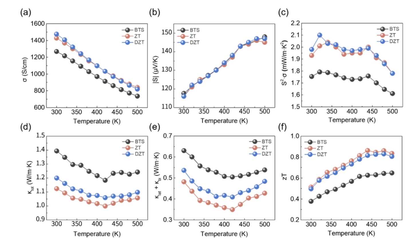
- The temperature-dependent thermoelectric properties are presented in Fig. 6. As shown in Fig. 6(a), the electrical conductivity of the coated specimens (both ZT and DZT) was higher than that of BTS over the entire temperature range and decreased with increasing temperature, characteristic of degenerate semiconductors; the enhancement reflects the increased carrier concentration and mobility. The Seebeck coefficient [Fig. 6(b)] was comparable among all specimens and increased with temperature. Consequently, the simultaneously enhanced electrical conductivity and preserved Seebeck coefficient yielded a markedly higher power factor for the ZT and DZT specimens than for BTS, with the DZT specimen showing the highest values in Fig. 6(c). The total thermal conductivity [Fig. 6(d)] was reduced in the coated specimens relative to BTS, and after subtracting the electronic contribution, the sum of lattice and bipolar thermal conductivity was lowest for the coated specimens. This result indicates that the dense, continuous oxide interfaces effectively scatter phonons as shown in Fig. 6(e). The electronic contribution subtracted here was evaluated with a constant Lorenz number of 2.44 × 10⁻⁸ W Ω K−2 (degenerate limit). Because the same value was applied to all three specimens, which were measured under identical conditions, the relative comparison in Fig. 6(e) is unaffected by this choice, although a systematic offset in the absolute values cannot be excluded at the higher measurement temperatures, where the bipolar contribution makes the degenerate approximation less accurate. As a result of the enhanced power factor and reduced thermal conductivity, the ZT and DZT specimens reached comparable zT values within the measurement uncertainty, both substantially exceeding that of uncoated BTS, with the ZT specimen showing the higher peak value and a broad maximum in the 420–460 K range [Fig. 6(f)]. These results demonstrate that the multilayer core-shell design simultaneously improves the electronic and phononic transport, thereby decoupling the conventional trade-off between the electrical and thermal transport. Taken together, the stronger core-level shifts of the DZT specimen (Fig. 2), its higher carrier concentration and effective mass (Fig. 5), and the comparable total shell thickness of the two coated specimens (Fig. 3) consistently indicate that the interfacial state of the two coating configurations genuinely differs, although the specific layered geometry responsible for this difference has not been directly imaged in the present work.
3. Results and Discussion
- In this study, a multilayer core-shell structure was realized by conformally coating BTS powders with ZnO-TiO2 oxide layers via rotary-type pALD and consolidating them by SPS. ED-XRF, HRSEM, XPS, and Cs-STEM analyses confirmed that uniform amorphous oxide shells approximately 4 nm thick were deposited on the powders without altering the particle morphology, and that these shells were retained as continuous, thermally stable interfacial films throughout the sintered body. The oxide interfaces donated electrons to the BTS matrix, increasing the carrier concentration and effective mass while maintaining the carrier mobility, which together enhanced the electrical conductivity and power factor. At the same time, the dense and continuous interfaces promoted phonon scattering, effectively reducing the lattice thermal conductivity. While the DZT specimen, prepared with a subdivided ZnO-TiO2 deposition sequence, achieved the highest power factor among the samples, the ZT specimen exhibited the lowest thermal conductivity. As a result, the ZT and DZT specimens attained comparable zT values within the measurement uncertainty, both markedly exceeding that of uncoated BTS, with the ZT specimen showing the higher peak value. These findings demonstrate that multilayer interface engineering via pALD is an effective strategy for simultaneously tuning the charge- and phonon-transport properties, offering a promising route to high-performance n-type Bi2Te3 thermoelectrics.
4. Conclusion
-
Funding
This work was supported by National Research Foundation of Korea (NRF) grants funded by the Korean Government (MSIT) (NRF-2023R1A2C1006831). This work was also supported by Korea Institute for Advancement of Technology (KIAT) grant funded by the Korea Government (MOTIR) (RS-2024-00409639, HRD Program for Industrial Innovation).
-
Conflict of Interest
The authors have no conflicts of interest to declare.
-
Data Availability Statement
All dataset files used in this study will be made available from the corresponding author upon reasonable request.
-
Author Information and Contribution
Su Min Eun: MSc; Conceptualization, Investigation, Validation, Visualization, Writing–original draft
Jin Kyeong Shin: MSc; Validation, Writing–review & editing
Se Been Jeong: Undergraduate; Validation, Writing–review & editing
Eui Seon Lee: PhD candidate; Resources, Writing–review & editing
Sung-Tag Oh; Professor; Resources, Writing–review & editing
Byung Joon Choi: Professor; Conceptualization, Resources, Funding acquisition, Supervision, Writing–review & editing
-
Acknowledgments
None.
Article information
| Element | Atomic concentration (%) | ||
|---|---|---|---|
| BTS | ZT | DZT | |
| Zn | - | 0.21 | 0.29 |
| Ti | - | 0.27 | 0.31 |
| O | 28.9 | 43.1 | 32.8 |
| BTS | 71.1 | 56.5 | 66.6 |
- 1. M. A. Okirigiti, C. M. Kim, H. Choi, N. R. Alluri and K.-I. Park: J. Powder Mater., 32 (2025) 1.ArticlePDF
- 2. J. Bae, S. Jo and K. T. Kim: J. Powder Mater., 30 (2023) 318.Article
- 3. S. Lee, T. J. Park and S. K. Kim: J. Powder Mater., 29 (2022) 56.Article
- 4. Z. Li, C. Xiao and Y. Xie: Appl. Phys. Rev., 9 (2022) 011303.Article
- 5. L. B. Vu, S. Jung, J. Bae, J. M. Park, K. T. Kim, I. Son and S. Jo: J. Powder Mater., 31 (2024) 119.ArticlePDF
- 6. Y. S. Lim and G.-G. Lee: J. Powder Mater., 31 (2024) 50.ArticlePDF
- 7. D. Champier: Energy Convers. Manag., 140 (2017) 167.Article
- 8. T. Zhu, Y. Liu, C. Fu, J. P. Heremans, G. J. Snyder and X. Zhao: Adv. Mater., 29 (2017) 1605884.Article
- 9. Z. Bu, X. Zhang, Y. Hu, Z. Chen, S. Lin, W. Li, C. Xiao and Y. Pei: Nat. Commun., 13 (2022) 237.Article
- 10. I. T. Witting, T. C. Chasapis, F. Ricci, M. Peters, N. A. Heinz, G. Hautier and G. J. Snyder: Adv. Electron. Mater., 5 (2019) 1800904.Article
- 11. P. Dharmaiah, S.-J. Jung, J.-S. Kim, S. K. Kim and S.-H. Baek: Appl. Phys. Rev., 11 (2024) 031312.Article
- 12. D. Teweldebrhan, V. Goyal and A. A. Balandin: Nano Lett., 10 (2010) 1209.Article
- 13. R. Orru, R. Licheri, A. M. Locci, A. Cincotti and G. Cao: Mater. Sci. Eng. R, 63 (2009) 127.Article
- 14. Y. Pei, H. Wang and G. J. Snyder: Adv. Mater., 24 (2012) 6125.Article
- 15. K.-C. Kim, S.-S. Lim, S. H. Lee, J. Hong, D.-Y. Cho, A. Y. Mohamed, C. M. Koo, S.-H. Baek, J.-S. Kim and S. K. Kim: ACS Nano, 13 (2019) 7146.Article
- 16. S. He, A. Bahrami, X. Zhang, I. G. Martinez, S. Lehmann and K. Nielsch: Adv. Mater. Technol., 7 (2022) 2100953.Article
- 17. G. M. Park, S. Lee, T. J. Park, S.-H. Baek, J.-S. Kim and S. K. Kim: Adv. Mater. Interfaces, 12 (2025) 2400581.Article
- 18. M. J. Jung, J. Y. Park, S. M. Eun and B. J. Choi: J. Powder Mater., 30 (2023) 130.Article
- 19. M. J. Jung, S. M. Eun, H. Kim, S. K. Kim, J. Byun and B. J. Choi: Kor. J. Chem. Eng., 42 (2025) 3545.ArticlePDF
- 20. S. E. Jung, J. W. Shin, Y. J. Han and B. J. Choi: J. Powder Mater., 32 (2025) 179.ArticlePDF
- 21. M. J. Jung, Y. J. Yun, J. Byun and B. J. Choi: J. Powder Mater., 28 (2021) 239.Article
- 22. M. J. Jung, M. Ji, J. H. Han, Y.-I. Lee, S.-T. Oh, M. H. Lee and B. J. Choi: Ceram. Int., 48 (2022) 36773.Article
- 23. S. M. Eun, E. S. Lee, J. K. Shin, S.-T. Oh and B. J. Choi: Microstructures, 6 (2026) 2026065.Article
- 24. S. M. Eun, E. S. Lee, S.-T. Oh, C. Jung and B. J. Choi: J. Materiomics, 12 (2026) 101279.
- 25. J. K. Shin, Y. Choi and B. J. Choi: J. Powder Mater., 33 (2026) 221.ArticlePDF
- 26. J. Y. Park, S. M. Eun, J. Byun and B. J. Choi: J. Powder Mater., 31 (2024) 255.ArticlePDF
- 27. H. Wang, S. Bai, L. Chen, A. Cuenat, G. Joshi, H. Kleinke, J. Konig, H. W. Lee, J. Martin, M.-W. Oh, W. D. Porter, Z. Ren, J. Salvador, J. Sharp, P. Taylor, A. J. Thompson and Y. C. Tseng: J. Electron. Mater., 44 (2015) 4482.ArticlePDF
- 28. Y.-X. Chen, Z.-H. Ge, M. Yin, D. Feng, X.-Q. Huang, W. Zhao and J. He: Adv. Funct. Mater., 26 (2016) 6836.Article
- 29. H. Wang, R. Gurunathan, C. Fu, R. Cui, T. Zhu and G. J. Snyder: Mater. Adv., 3 (2022) 734.Article
References
Figure & Data
References
Citations

 ePub Link
 Cite this Article
 XML Download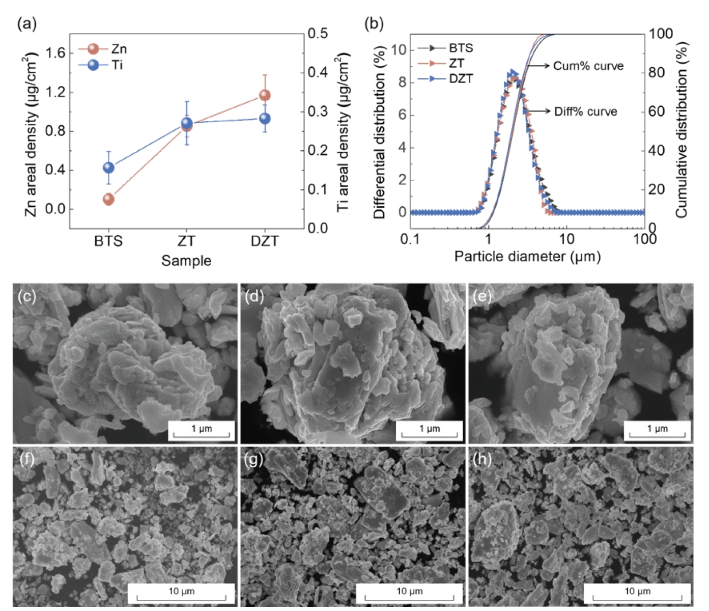
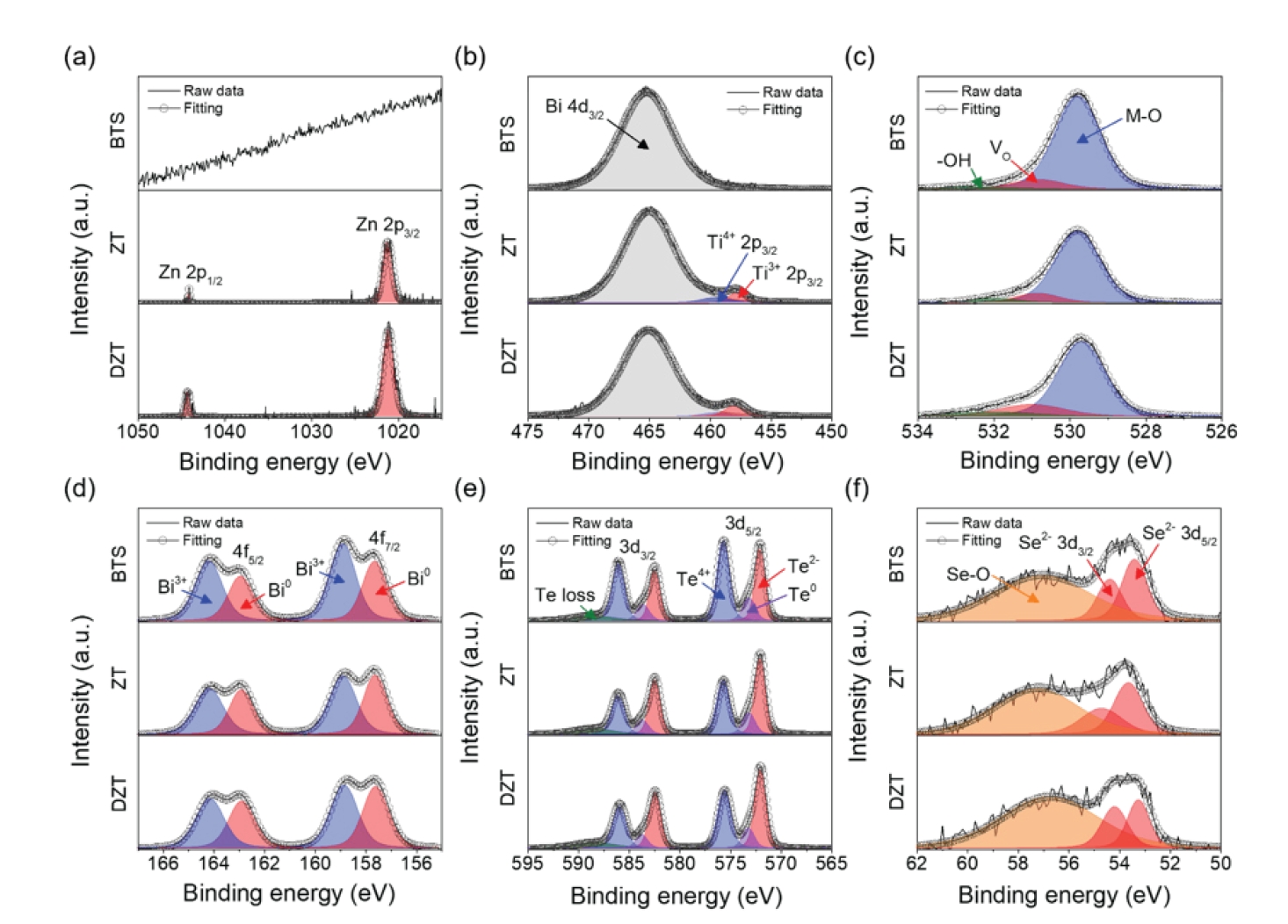
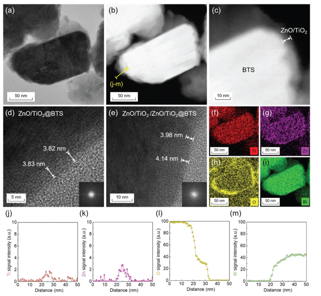
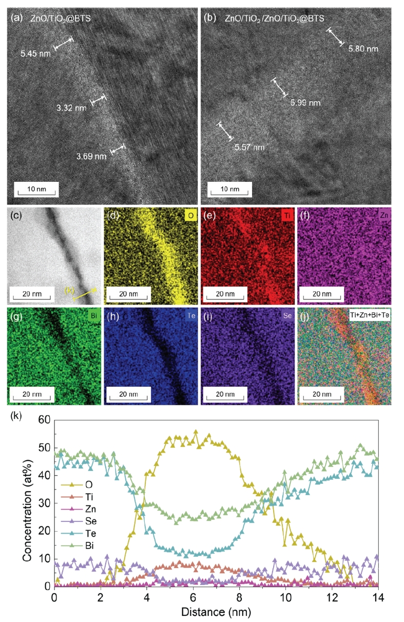
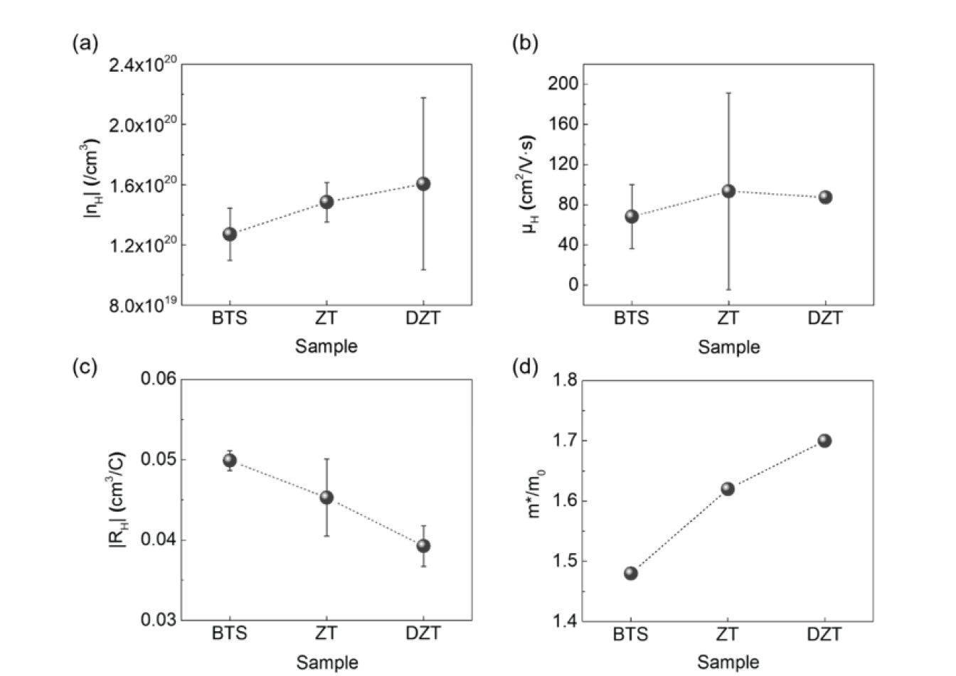
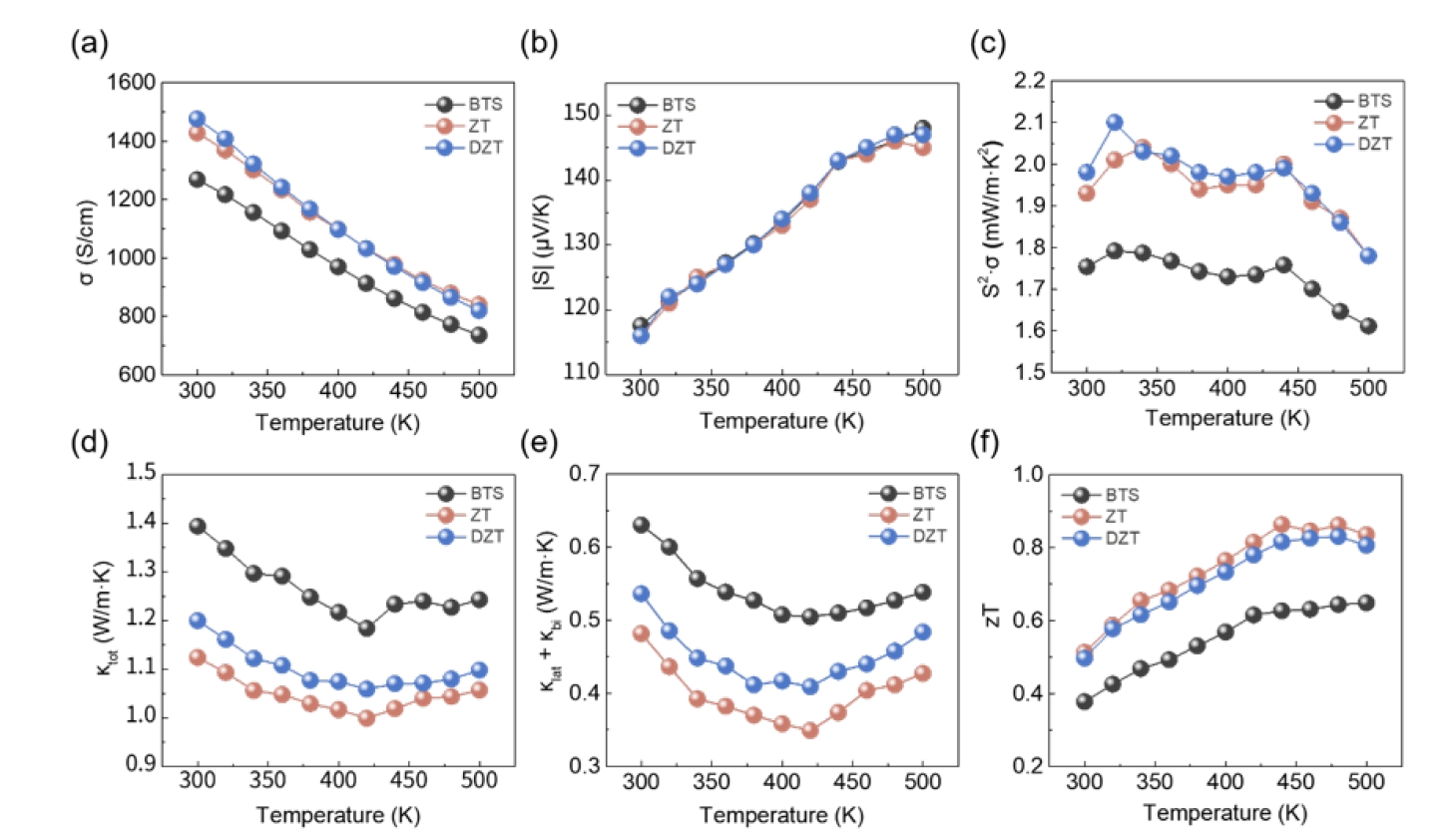
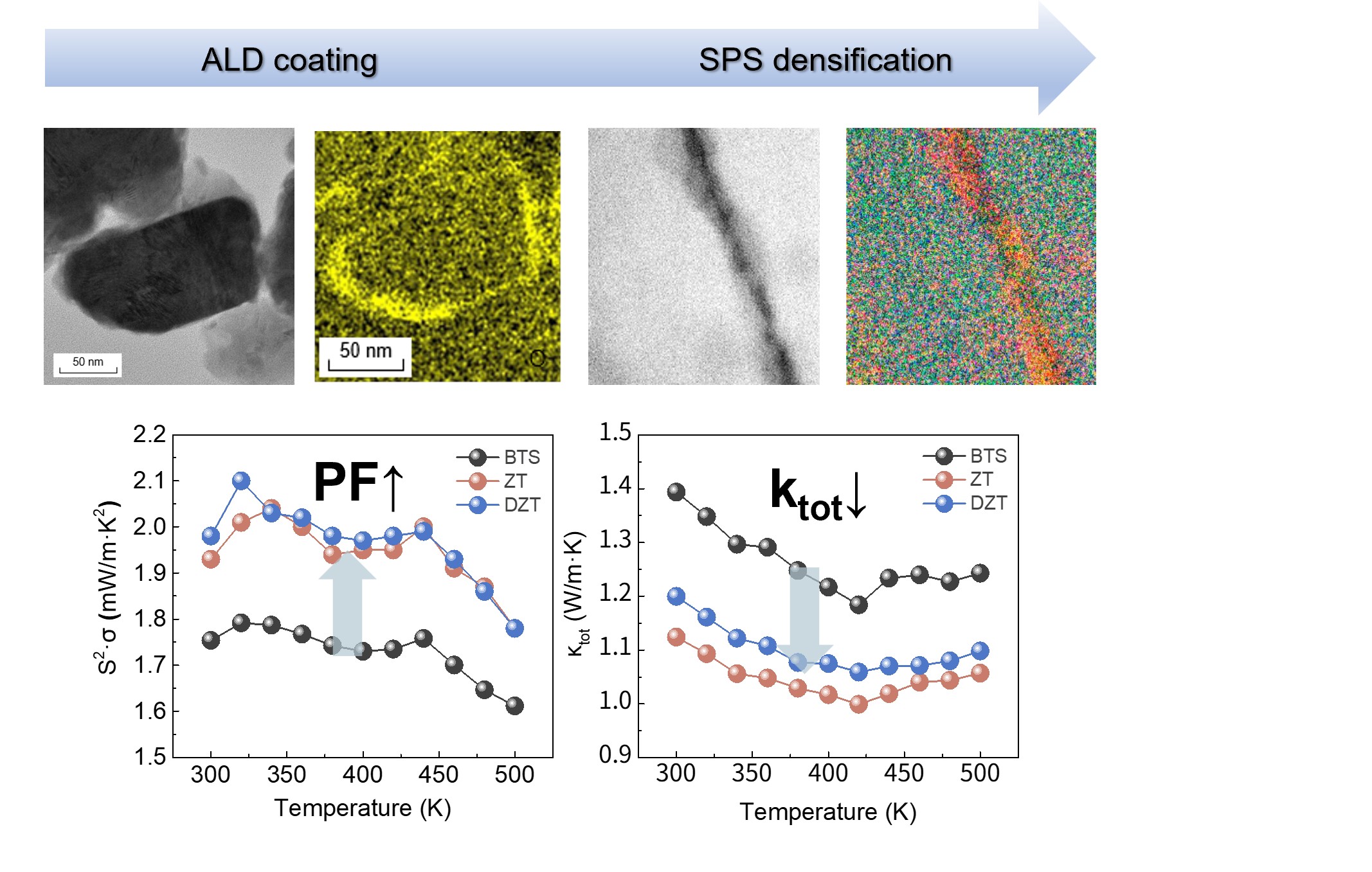







Fig. 1.
Fig. 2.
Fig. 3.
Fig. 4.
Fig. 5.
Fig. 6.
Graphical abstract
| Element | Atomic concentration (%) | ||
|---|---|---|---|
| BTS | ZT | DZT | |
| Zn | - | 0.21 | 0.29 |
| Ti | - | 0.27 | 0.31 |
| O | 28.9 | 43.1 | 32.8 |
| BTS | 71.1 | 56.5 | 66.6 |
Table 1.
TOP

