
Search
- Page Path
- HOME > Search
- [Korean]
- Fabrication, Microstructure and Adhesion Properties of BCuP-5 Filler Metal/Ag Plate Clad Material by Using High Velocity Oxygen Fuel Thermal Spray Process
- Yeun A Joo, Yong-Hoon Cho, Jae-Sung Park, Kee-Ahn Lee
- J Powder Mater. 2022;29(3):226-232. Published online June 1, 2022
- DOI: https://doi.org/10.4150/KPMI.2022.29.3.226
- 1,330 View
- 4 Download
-
 Abstract
 PDF
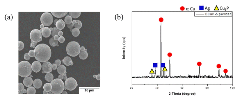
PDF In this study, a new manufacturing process for a multilayer-clad electrical contact material is suggested. A thin and dense BCuP-5 (Cu-15Ag-5P filler metal) coating layer is fabricated on a Ag plate using a high-velocity oxygen-fuel (HVOF) process. Subsequently, the microstructure and bonding properties of the HVOF BCuP-5 coating layer are evaluated. The thickness of the HVOF BCuP-5 coating layer is determined as 34.8 μm, and the surface fluctuation is measured as approximately 3.2 μm. The microstructure of the coating layer is composed of Cu, Ag, and Cu-Ag-Cu3P ternary eutectic phases, similar to the initial BCuP-5 powder feedstock. The average hardness of the coating layer is 154.6 HV, which is confirmed to be higher than that of the conventional BCuP-5 alloy. The pull-off strength of the Ag/BCup-5 layer is determined as 21.6 MPa. Thus, the possibility of manufacturing a multilayer-clad electrical contact material using the HVOF process is also discussed.
- [Korean]
- Fabrication, Microstructure and Adhesive Properties of BCuP-5 Filler Metal/Ag Plate Composite by using Plasma Spray Process
- Seong-June Youn, Young-Kyun Kim, Jae-Sung Park, Joo-Hyun Park, Kee-Ahn Lee
- J Korean Powder Metall Inst. 2020;27(4):333-338. Published online August 1, 2020
- DOI: https://doi.org/10.4150/KPMI.2020.27.4.333
- 999 View
- 3 Download
-
Abstract
PDF
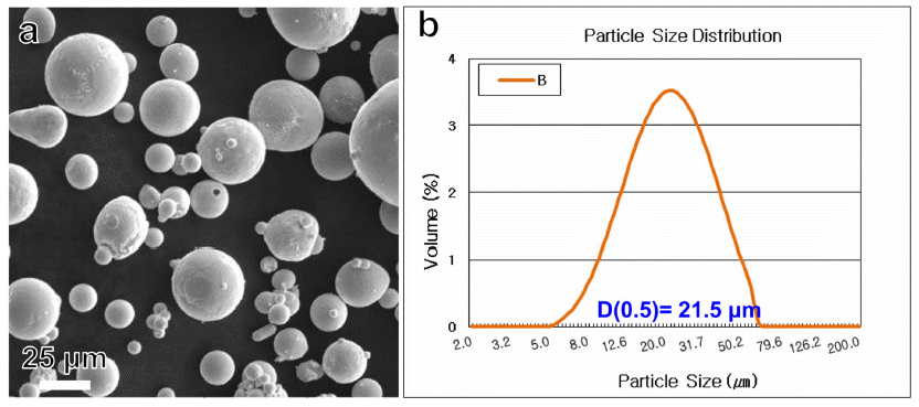
In this study, we fabricate a thin- and dense-BCuP-5 coating layer, one of the switching device multilayers, through a plasma spray process. In addition, the microstructure and macroscopic properties of the coating layer, such as hardness and bond strength, are investigated. Both the initial powder feedstock and plasma-sprayed BCuP-5 coating layer show the main Cu phase, Cu-Ag-Cu3P ternary phases, and Ag phase. This means that microstructural degradation does not occur during plasma spraying. The Vickers hardness of the coating layer was measured as 117.0 HV, indicating that the fine distribution of the three phases enables the excellent mechanical properties of the plasma-sprayed BCuP-5 coating layer. The pull-off strength of the plasma-sprayed BCuP-5 coating layer is measured as 16.5 kg/cm2. Based on the above findings, the applicability of plasma spray for the fabrication process of low-cost multi-layered electronic contact materials is discussed and suggested.
- [Korean]
- Thermal Properties of Diamond Aligned Electroless Ni Plating Layer/Oxygen Free Cu Substrates
- Da-Woon Jeong, Song-Yi Kim, Kyoung-Tae Park, Seok-Jun Seo, Taek Soo Kim, Bum Sung Kim
- J Korean Powder Metall Inst. 2015;22(2):134-137. Published online April 1, 2015
- DOI: https://doi.org/10.4150/KPMI.2015.22.2.134
- 1,345 View
- 8 Download
-
Abstract
PDF
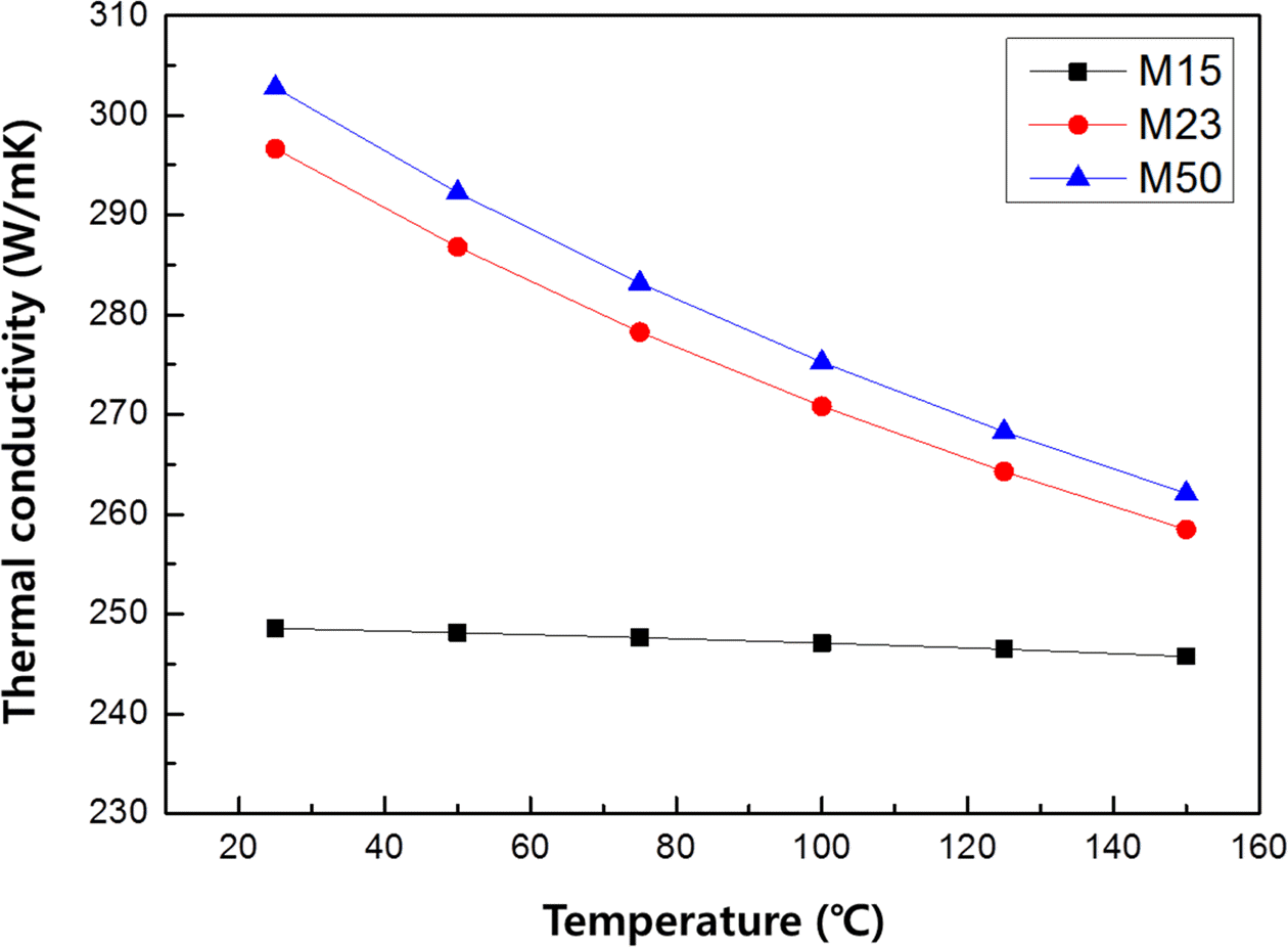
The monolayer engineering diamond particles are aligned on the oxygen free Cu plates with electroless Ni plating layer. The mean diamond particle sizes of 15, 23 and 50 μm are used as thermal conductivity pathway for fabricating metal/carbon multi-layer composite material systems. Interconnected void structure of irregular shaped diamond particles allow dense electroless Ni plating layer on Cu plate and fixing them with 37-43% Ni thickness of their mean diameter. The thermal conductivity decrease with increasing measurement temperature up to 150°C in all diamond size conditions. When the diamond particle size is increased from 15 μm to 50 μm (Max. 304 W/mK at room temperature) tended to increase thermal conductivity, because the volume fraction of diamond is increased inside plating layer.
 First
First Prev
Prev

TOP
