
Articles
- Page Path
- HOME > J Korean Powder Metall Inst > Volume 24(4); 2017 > Article
-
ARTICLE
- Development of Dark Field image Processing Technique for the Investigation of Nanostructures
- Jongchul Jeon, Kyou-Hyun Kim*
-
Journal of Korean Powder Metallurgy Institute 2017;24(4):285-291.
DOI: https://doi.org/10.4150/KPMI.2017.24.4.285
Published online: July 31, 2017
Manufacturing Technology Office, Korea Institute for Rare Metal, Korea Institute of Industrial Technology,Incheon 21999, Republic of Korea
- *Corresponding Author: Kyou-Hyun Kim, +82-32-850-0431, +82-32-850-0430, khkim1308@kitech.re.kr
• Received: August 12, 2017 • Revised: August 19, 2017 • Accepted: August 21, 2017
© The Korean Powder Metallurgy Institute. All rights reserved.
- 1,630 Views
- 3 Download
Abstract
- We propose a custom analysis technique for the dark field (DF) image based on transmission electron microscopy (TEM). The custom analysis technique is developed based on the DigitalMicrograph® (DM) script language embedded in the Gatan digital microscopy software, which is used as the operational software for most TEM instruments. The developed software automatically scans an electron beam across a TEM sample and records a series of electron diffraction patterns. The recorded electron diffraction patterns provide DF and ADF images based on digital image processing. An experimental electron diffraction pattern is recorded from a IrMn polycrystal consisting of fine nanograins in order to test the proposed software. We demonstrate that the developed image processing technique well resolves nanograins of ~ 5 nm in diameter.
- Conventional TEM (transmission electron microscopy) analysis techniques have been drastically improved based on the advance on TEM instrument such as aberration correctors and ultra-fast charge-coupled device (CCD) camera. Such development provides a real atomic resolution image with the scanning TEM technique (STEM). The ultra-fast CCD camera records real time images for in-situ observation. On the other hand, numerous custom analysis techniques have been developed in an effort to obtain concealed information, which is hardly distinguishable by conventional methods or manual calculations [1- 6]. For example, strain mapping software is introduced based on geometric phase analysis (GPA) or peak-pair analysis (PPA) technique [5, 6].
- Custom image processing techniques are in general developed using conventional programming languages, such as C/C++, Fortran, Matlab, and Python. Advantage of using these programming languages is fast calculation time to process TEM images. On the other hand, the custom TEM control is impossible because most operational TEM software does not provide a communication link between TEM instrument and the programming languages of C/C++, Fortran, Matlab, and Python. Unlike other programming languages, DigitalMicrograph® (DM, Gatan Inc.) script language embeded in the Gatan digital microscopy software gives a variety of simple functions to manipulate TEM images and to access the TEM instrument. The DM scripting language features a simplified programming language based on the very similar syntax of other programming languages. DM script works as an interpreter by simultaneously working as a compiler to create an object file, as a linker to create an executable file, and as a runtime environment. Since DM acts as an interpreter, its computation speed is relatively slow comparing to other low-level languages. Nevertheless, an electron microscope can be directly operated using DM script by communicating with the host processor built-in inside TEM and with the correct microscope control plug-in installed. The custom TEM control then provides a lot of new methods to investigate nanostructures.
- In this study, we propose a digital image processing script for dark field (DF) imaging and annular dark field (ADF) imaging. In conventional dark field (DF) image, an aperture is used to block a direct beam and to select one or more diffracted electron beams. Then, the selected diffracted electrons only pass an objective aperture to form an image. This technique is powerful to investigate stacking faults, defects or phase distribution. The conventional DF image, however, has the limitations such as very low intensity level of recorded image or limited aperture size to select the diffracted electron beam. For the conventional ADF imaging, an annular detector is used to collect diffracted electron beams. This technique is widely used for Z-contrast imaging with a high-angle annular-dark field (HAADF) detector. In Z-contrast image, image contrast mainly depends on the atomic mass. On the other hand, low-angle annular dark-field image is used to investigate a specimen composed of light elements. Like the DF imaging, however, ADF image uses a strongly focused electron beam so that the specimen is often damaged.
- To overcome the conventional limitations of ADF and DF imaging techniques we develop an algorithm of digital image processing for ADF imaging with the proposed scanning electron diffraction technique. The proposed algorithm provides DF and ADF imaging technique. We applied the developed script to a IrMn polycrystal having very fine nanograins of few nanometer in diameter. The results show that the proposed algorithm is well resolve each nanograin without causing any damages on the sample.
Introduction
- 2.1. TEM control for scanning diffraction
- The electron beam is automatically controlled based on the DM script language. Table 1 shows the main functions for scanning electron diffraction (SED). Two commands of EMGetBeamShift and EMSetBeamShift are used to position the electron beam. The first command of EMGet- BeamShift read and save the current values of beam shift coils into the real number x and y. The values of x and y, however, only refer to the unitless values of electromagnetic lenses so that the values need to be converted into a real unit such as nanometer or micrometer. Details of converting procedures can be found in the previous study [7]. The series of diffraction patterns (DP) are automatically acquired during beam scanning for the DF and ADF imaging. SSCGainNormalizedBinnedAcquire command is used for automatic acquisition process. The recorded DP patterns are then saved into a multilayered image.
- 2.2. Image analysis for the scanning diffraction data set
- Figure 1 shows the imaging processing procedures for ADF and DF imaging. For the ADF imaging, two oval annotations (red circles) are first used to define the area as shown in Fig. 1(a). Next, an annular mask image is created for the calculation (Fig. 1(b)). The annular mask image consists of the white area with the intensity of 1 and the black area with the intensity of 0. Then, the final template is obtained by multiplying the mask image to the original image as shown in Fig. 1(c). Figure 1(d-f) shows the algorithm for the DF imaging. The DF imaging uses one oval annotation (Fig. 1(d)). Like the ADF imaging, the final template (Fig. 1(f)) is obtained by multiplying the mask image (Fig. 1(e)) to the original image. Using the final template, the ADF and DF image are calculated by the sum of intensity values inside the selected area.
- 2.3. ADF and DF imaging script
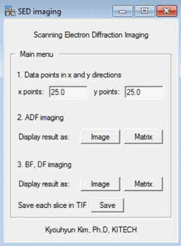
- Figure 2 shows the ADF and DF imaging software installed on the Gatan digital microscopy software. The script source listing can be found in the Appendix. As shown in Fig. 1, the dialog box consists of input values for recorded image information, ADF imaging menu, and DF (or BF) imaging menu.
The Program
Table 1
TEM control commands for scanning electron diffraction

- We use a IrMn polycrystal to demonstrate our image processing technique for the ADF and DF imaging. Figure 3(a) shows the typical bright field image recorded from the IrMn polycrystal. The IrMn consists of very fine nanograins of <20 nm in diameter so that the specimen is proper to test the developed software. For the ADF imaging, the electron beam of 5 nm in diameter scans the IrMn sample (Fig. 3(a)) over the area of 75 × 75 nm2. Total acquisition data points are 15 × 15 rectangular grids along the x and y direction and the distance between the acquisition points is 5 nm. A series of electron diffraction patterns are stored in a dataset during the beam scanning process [1]. The ADF image is then calculated for the annular area between 8.387 nm-1 and 11.936 nm-1 as indicated by the arrows in Fig. 3(b). Figure 3(c) shows the calculated ADF image for the selected annular area. In the calculated ADF image, the bright regions (yellow circles in Fig. 2(c)) correspond to the dark region in Fig. 2(a). This indicates that the nanograins indicated by the yellow circles in Fig. 2(a) has the lattice parameters between 1.676 Å and 2.384 Å. In addition, the circled nanograins have almost same intensity so that they are considered as a same phase and orientation. This result shows that the developed software precisely resolve the nanograins of 5~15 nm in diameter.
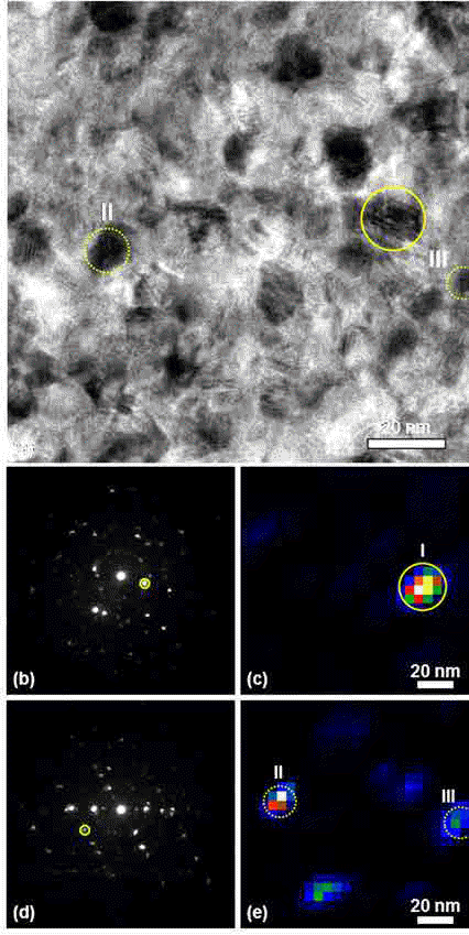
- The DF imaging technique is also applied to the IrMn specimen (Fig. 4(a)). For the DF imaging, 25 × 25 data points are used to record a series of electron diffraction patterns. The distance between acquisition points is 5 nm so that the total scanned area is 125 × 125 nm2. Like the ADF imaging, the electron beam size is 5 nm in diame- ter. The DF image is calculated for two different diffracted spots as shown in Figs. 4(b) and (d). Figures 4(c) and (e) show the calculated DF images for the selected spots. Based on the calculated DF image, the complex microstructure shown in Fig. 4(a) is well resolved even for the nanograins of 5 nm in diameter. In addition, the phase or orientation can be investigated using the developed software.
Experimental results
Fig. 3
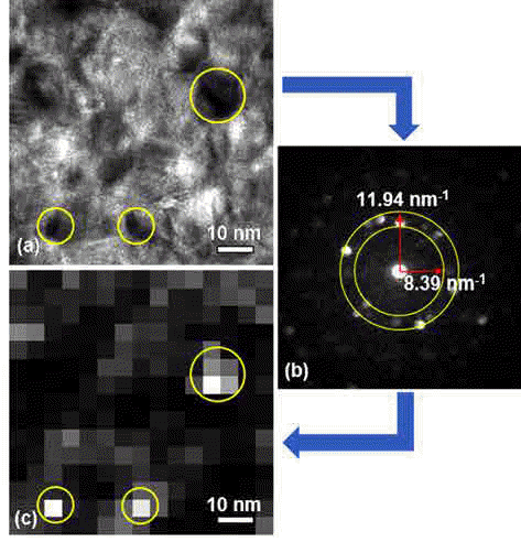
(a) Typical microstructure of IrNm polycrystal, (b) scanning electron diffraction data set obtained from (a) and (c) the calculated ADF image.
- We have proposed the script source for ADF and DF imaging process based on the DM script. For the test, the IrMn polycrystal is used to test the developed software. The result shows that the proposed digital image processing technique well resolve the nanograins even up to 5 nm in diameter, which is hardly achievable using the conventional TEM techniques. The conventional TEM technique for DF imaging is limited by the aperture size while the proposed image processing technique is in principle free to a selection size. In addition, the developed DF image processing technique gives very high intensity to understand an image contrast while the conventional DF imaging process is hard to obtain clear image contrast. Also, the quick scanning procedure prevent causing any damages on the TEM sample so that the original sample structure can be preserved. This study is of importance to propose the digital image processing technique for ADF and DF with the broad applications of precise microstructural study for nanostructure such as noanograin and nanopoweder.
Conclusion
-
Acknowledgements
- This work was supported by a research grant from the Korea Institute of Industrial Technology (KITECH).
Acknowledgement
- 1. K.H. Kim and J.M. Zuo: Ultramicroscopy., (2013) 124 71.Article
- 2. K.H. Kim: Appl. Microsc., (2015) 45 101.Article
- 3. J.M. Zuo, I. Vartanyants, M. Gao, R. Zhang and L. Nagahara: Science., (2003) 300 1419.Article
- 4. H. Kim, Y. Meng, J.L. Rouviére, D. Isheim, D.N. Seidman and J. Min Zuo: J. Appl. Phys., (2013) 113 103511.
- 5. M. Hÿtch, E. Snoeck and R. Kilaas: Ultramicroscopy., (1998) 74 131.Article
- 6. P. Galindo, S. Kret, A. Sanchez, J.Y. Laval, A. Andrés, J. Pizarro, E. Guerrero, T. Ben and S. Molina: Ultramicroscopy., (2007) 107 1186.Article
- 7. K.H. Kim, H. Xing, J.M. Zuo and H. Wang: Micron., (2015) 71 39.Article
Figure & Data
References
Citations
Citations to this article as recorded by 
 Cite this Article
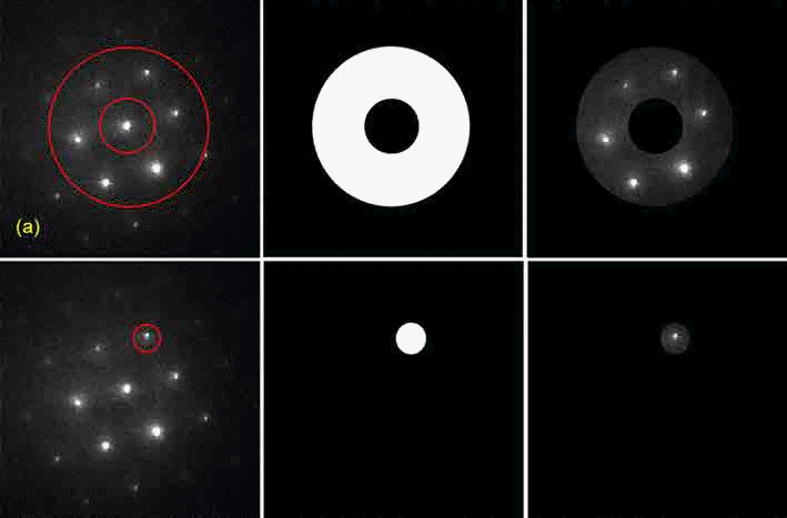


Development of Dark Field image Processing Technique for the Investigation of Nanostructures


Fig. 1
Image processing procedures used for (a, b, c) ADF and (d, e, f) DF imaging.
Fig. 2
Developed ADF and DF imaging software installed on the Gatan digital microscopy software.
Fig. 3
(a) Typical microstructure of IrNm polycrystal, (b) scanning electron diffraction data set obtained from (a) and (c) the calculated ADF image.
Fig. 4
Calculated DF images from the scanning electron diffraction patterns recorded from the IrMn polycrystal.
Fig. 1
Fig. 2
Fig. 3
Fig. 4
Development of Dark Field image Processing Technique for the Investigation of Nanostructures
| Synopsis | EMGetBeamShift (Number x, Number y) |
| Description | Retrieve the value of beam shift coil and assign to the number of x and y |
| Synopsis | EMSetBeamShift (Number x, Number y) |
| Description | Shift the beam by the amounts of x and y |
| Synopsis | SSCGainNormalizedBinnedAcquire (Image, Exposure, Binning, top, left, bottom, right) |
| Description | Acquire an gain normalized SSC frame |
Table 1
TEM control commands for scanning electron diffraction
Table 1
TOP
