
Search
- Page Path
- HOME > Search
- [English]
- Recent Advances in Thermoelectric Materials and Devices: Improving Power Generation Performance
- Momanyi Amos Okirigiti, Cheol Min Kim, Hyejeong Choi, Nagamalleswara Rao Alluri, Kwi-Il Park
- J Powder Mater. 2025;32(1):1-15. Published online February 28, 2025
- DOI: https://doi.org/10.4150/jpm.2024.00395
- 10,606 View
- 235 Download
- 6 Citations
-
 Abstract
 PDF
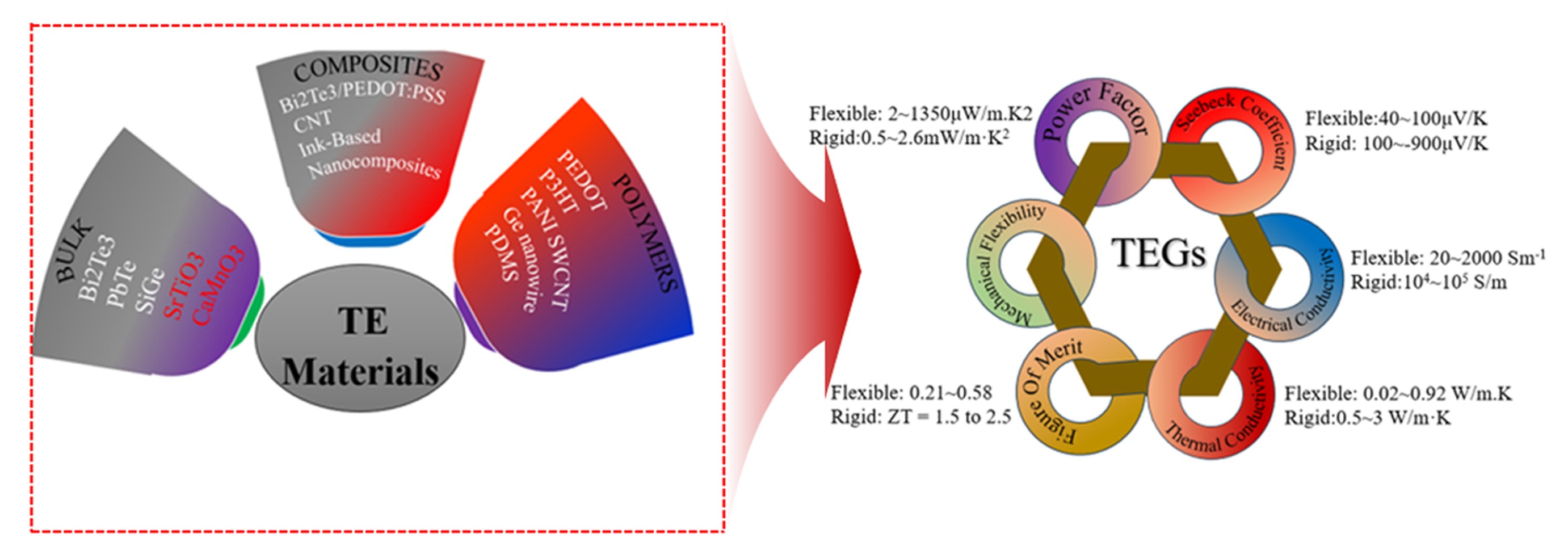
PDF - Thermoelectric materials have been the focus of extensive research interest in recent years due to their potential in clean power generation from waste heat. Their conversion efficiency is primarily reflected by the dimensionless figure of merit, with higher values indicating better performance. There is a pressing need to discover materials that increase output power and improve performance, from the material level to device fabrication. This review provides a comprehensive analysis of recent advancements, such as Bi2Te3-based nanostructures that reduce thermal conductivity while maintaining electrical conductivity, GeTe-based high entropy alloys that utilize multiple elements for improved thermoelectric properties, porous metal-organic frameworks offering tunable structures, and organic/hybrid films that present low-cost, flexible solutions. Innovations in thermoelectric generator designs, such as asymmetrical geometries, segmented modules, and flexible devices, have further contributed to increased efficiency and output power. Together, these developments are paving the way for more effective thermoelectric technologies in sustainable energy generation.
-
Citations
Citations to this article as recorded by
- State-of-the-art research in conducting polymer thermoelectric composites: Design strategies, doping innovations, and emerging technologies
Vilakshana Acharya, Shivani Verma, Seema Gupta, Gaurav Pandey, Aanchal Sethi, Pooja Rawat
Journal of Applied Physics.2026;[Epub] CrossRef - Mathematical and simulation modeling of photovoltaic systems utilizing thermoelectric modules for effective thermal management
Muhammad Sohaib Tahir, Xue Dong, Muhammad Mansoor Khan
Results in Engineering.2025; 27: 106344. CrossRef - Summary of Publications in the Special Issue: Advances in Corrosion Resistant Coatings
Yong X. Gan
Coatings.2025; 15(11): 1350. CrossRef - Standard Reference Thermoelectric Modules Based on Metallic Combinations and Geometric Design
EunA Koo, Hanhwi Jang, SuDong Park, Sang Hyun Park, Sae-byul Kang
Applied Sciences.2025; 15(18): 10273. CrossRef - Research Trends in Magneto-Mechano-Electric (MME) Energy Harvesting Devices
So Ie Jeong, Geon-Tae Hwang
Journal of Powder Materials.2025; 32(6): 529. CrossRef - Transient In-Situ Identification of Thermal Parameters in Commercial Thermoelectric Modules using Transfer-Function Models
Gurum Ahmad Pauzi, Irfan Alfiansyah, Agus Riyanto, Donni Kis Apriyanto, Yanti Yulianti, Warsito Warsito
Jurnal Ilmiah Pendidikan Fisika Al-Biruni.2025; 14(2): 187. CrossRef
- State-of-the-art research in conducting polymer thermoelectric composites: Design strategies, doping innovations, and emerging technologies
- [Korean]
- Fabrication of Nanowire by Electrospinning Process Using Nickel Oxide Particle Recovered from MLCC
- Haein Shin, Jongwon Bae, Minsu Kang, Kun-Jae Lee
- J Powder Mater. 2023;30(6):502-508. Published online December 1, 2023
- DOI: https://doi.org/10.4150/KPMI.2023.30.6.502
- 869 View
- 14 Download
- 1 Citations
-
Abstract
PDF
With the increasing demand for electronic products, the amount of multilayer ceramic capacitor (MLCC) waste has also increased. Recycling technology has recently gained attention because it can simultaneously address raw material supply and waste disposal issues. However, research on recovering valuable metals from MLCCs and converting the recovered metals into high-value-added materials remains insufficient. Herein, we describe an electrospinning (E-spinning) process to recover nickel from MLCCs and modulate the morphology of the recovered nickel oxide particles. The nickel oxalate powder was recovered using organic acid leaching and precipitation. Nickel oxide nanoparticles were prepared via heat treatment and ultrasonic milling. A mixture of nickel oxide particles and polyvinylpyrrolidone (PVP) was used as the E-spinning solution. A PVP/NiO nanowire composite was fabricated via Espinning, and a nickel oxide nanowire with a network structure was manufactured through calcination. The nanowire diameters and morphologies are discussed based on the nickel oxide content in the E-spinning solution.
-
Citations
Citations to this article as recorded by- Morphological Control and Surface Modification Characteristics of Nickel Oxalate Synthesized via Oxalic Acid Precipitation
Eunbi Park, Jongwon Bae, Sera Kang, Minsu Kang, Suseong Lee, Kun-Jae Lee
Journal of Powder Materials.2025; 32(5): 375. CrossRef
- Morphological Control and Surface Modification Characteristics of Nickel Oxalate Synthesized via Oxalic Acid Precipitation
- [Korean]
- Effect of Post Heat Treatment on the Microstructure and Mechanical Properties of BCuP-5 Filler Metal Coating Layers Fabricated by High Velocity Oxygen Fuel Thermal Spray Process on Ag Substrate
- So-Yeon Park, Seong-June Youn, Jae-Sung Park, Kee-Ahn Lee
- J Powder Mater. 2022;29(4):283-290. Published online August 1, 2022
- DOI: https://doi.org/10.4150/KPMI.2022.29.4.283
- 1,273 View
- 2 Download
- 1 Citations
-
Abstract
PDF
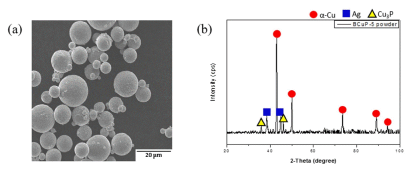
A Cu-15Ag-5P filler metal (BCuP-5) is fabricated on a Ag substrate using a high-velocity oxygen fuel (HVOF) thermal spray process, followed by post-heat treatment (300°C for 1 h and 400°C for 1 h) of the HVOF coating layers to control its microstructure and mechanical properties. Additionally, the microstructure and mechanical properties are evaluated according to the post-heat treatment conditions. The porosity of the heat-treated coating layers are significantly reduced to less than half those of the as-sprayed coating layer, and the pore shape changes to a spherical shape. The constituent phases of the coating layers are Cu, Ag, and Cu-Ag-Cu3P eutectic, which is identical to the initial powder feedstock. A more uniform microstructure is obtained as the heat-treatment temperature increases. The hardness of the coating layer is 154.6 Hv (as-sprayed), 161.2 Hv (300°C for 1 h), and 167.0 Hv (400°C for 1 h), which increases with increasing heat-treatment temperature, and is 2.35 times higher than that of the conventional cast alloy. As a result of the pull-out test, loss or separation of the coating layer rarely occurs in the heat-treated coating layer.
-
Citations
Citations to this article as recorded by- Evaluation and Prediction of Mechanical Properties According to Welding Methods of Ni 825/A516-70N Clad Plates
Cheolhong Hwang, Jeongseok Oh, Jini Park, Myungwoo Joe, Sunhwan Kim, Kyunghoon Yoo, Sungwoong Kim, Youngjoo Kim, Sangyeob Lee, Joonsik Park
Korean Journal of Metals and Materials.2024; 62(11): 844. CrossRef
- Evaluation and Prediction of Mechanical Properties According to Welding Methods of Ni 825/A516-70N Clad Plates
- [Korean]
- Fabrication, Microstructure and Adhesion Properties of BCuP-5 Filler Metal/Ag Plate Clad Material by Using High Velocity Oxygen Fuel Thermal Spray Process
- Yeun A Joo, Yong-Hoon Cho, Jae-Sung Park, Kee-Ahn Lee
- J Powder Mater. 2022;29(3):226-232. Published online June 1, 2022
- DOI: https://doi.org/10.4150/KPMI.2022.29.3.226
- 1,037 View
- 4 Download
-
Abstract
PDF
In this study, a new manufacturing process for a multilayer-clad electrical contact material is suggested. A thin and dense BCuP-5 (Cu-15Ag-5P filler metal) coating layer is fabricated on a Ag plate using a high-velocity oxygen-fuel (HVOF) process. Subsequently, the microstructure and bonding properties of the HVOF BCuP-5 coating layer are evaluated. The thickness of the HVOF BCuP-5 coating layer is determined as 34.8 μm, and the surface fluctuation is measured as approximately 3.2 μm. The microstructure of the coating layer is composed of Cu, Ag, and Cu-Ag-Cu3P ternary eutectic phases, similar to the initial BCuP-5 powder feedstock. The average hardness of the coating layer is 154.6 HV, which is confirmed to be higher than that of the conventional BCuP-5 alloy. The pull-off strength of the Ag/BCup-5 layer is determined as 21.6 MPa. Thus, the possibility of manufacturing a multilayer-clad electrical contact material using the HVOF process is also discussed.
- [Korean]
- Fabrication, Microstructure and Adhesive Properties of BCuP-5 Filler Metal/Ag Plate Composite by using Plasma Spray Process
- Seong-June Youn, Young-Kyun Kim, Jae-Sung Park, Joo-Hyun Park, Kee-Ahn Lee
- J Korean Powder Metall Inst. 2020;27(4):333-338. Published online August 1, 2020
- DOI: https://doi.org/10.4150/KPMI.2020.27.4.333
- 809 View
- 3 Download
-
Abstract
PDF
In this study, we fabricate a thin- and dense-BCuP-5 coating layer, one of the switching device multilayers, through a plasma spray process. In addition, the microstructure and macroscopic properties of the coating layer, such as hardness and bond strength, are investigated. Both the initial powder feedstock and plasma-sprayed BCuP-5 coating layer show the main Cu phase, Cu-Ag-Cu3P ternary phases, and Ag phase. This means that microstructural degradation does not occur during plasma spraying. The Vickers hardness of the coating layer was measured as 117.0 HV, indicating that the fine distribution of the three phases enables the excellent mechanical properties of the plasma-sprayed BCuP-5 coating layer. The pull-off strength of the plasma-sprayed BCuP-5 coating layer is measured as 16.5 kg/cm2. Based on the above findings, the applicability of plasma spray for the fabrication process of low-cost multi-layered electronic contact materials is discussed and suggested.
- [Korean]
- Fabrication of Photoelectrochromic Devices Composed of Anodized TiO2 and WO3 Nanostructures
- Sanghoon Lee, Hyeongcheol Cha, Yoon-Chae Nah
- J Korean Powder Metall Inst. 2015;22(5):326-330. Published online October 1, 2015
- DOI: https://doi.org/10.4150/KPMI.2015.22.5.326
- 734 View
- 3 Download
- 3 Citations
-
Abstract
PDF
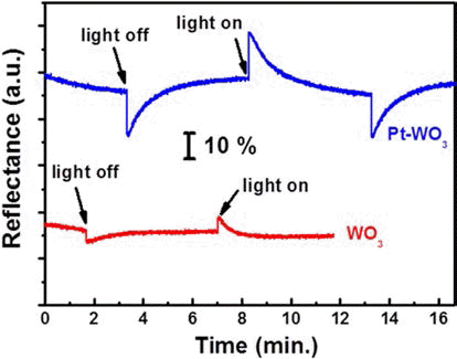
In this study, we demonstrate the photoelectrochromic devices composed of TiO2 and WO3 nanostructures prepared by anodization method. The morphology and the crystal structure of anodized TiO2 nanotubes and WO3 nanoporous layers are investigated by SEM and XRD. To fabricate a transparent photoelectrode on FTO substrate, a TiO2 nanotube membrane, which has been detached from Ti substrate, is transferred to FTO substrate and annealed at 450°C for 1 hr. The photoelectrode of TiO2 nanotube and the counter electrode of WO3 nanoporous layer are assembled and the inner space is filled with a liquid electrolyte containing 0.5 M LiI and 5 mM I2 as a redox mediator. The properties of the photoelectrochromic devices is investigated and Pt-WO3 electrode system shows better electrochromic performance compared toWO3 electrode.
-
Citations
Citations to this article as recorded by- Synthesis and characterization of nitrogen-doped TiO2 coatings on reduced graphene oxide for enhancing the visible light photocatalytic activity
Yifan Zhang, Hye Mee Yang, Soo-Jin Park
Current Applied Physics.2018; 18(2): 163. CrossRef - Photocatalytic and Adsorption Properties of WO3 Nanorods Prepared by Hydrothermal Synthesis
Su-Yeol Yu, Chunghee Nam
Journal of Korean Powder Metallurgy Institute.2017; 24(6): 483. CrossRef - Synthesis and Photo Catalytic Activity of 10 wt%, 20 wt%Li-TiO2 Composite Powders
Hyeong-Chul Kim, Jae-Kil Han
Journal of Korean Powder Metallurgy Institute.2016; 23(1): 33. CrossRef
- Synthesis and characterization of nitrogen-doped TiO2 coatings on reduced graphene oxide for enhancing the visible light photocatalytic activity
 First
First Prev
Prev

TOP
